

Opamp – Operational Amplifier
Contents
What is an Opamp ?
Opamp is the abbreviation of Operational Amplifier. An operational amplifier is a direct coupled high gain amplifier usually consisting of one or more differential amplifiers followed by a level transistor and an output stage. The output stage is generally push-pull or complementary symmetry push-pull amplifier.
Opamps are building blocks of analog circuitry and is also known as differential amplifier as its output depends on difference between input signals. It can also be used to amplify both DC as well as AC signals. Op-amp is primarily designed for old analog computers, where they were used for computing mathematical functions like addition, subtraction etc. By using suitable external feedback components opamp can be used for applications like amplifiers, oscillators, comparators etc.
What makes opamp different from other amplifiers ?
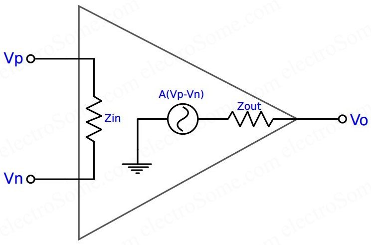
Opamp is a differential amplifier having very high gain. It has basically 2 inputs, non-inverting input (Vp or V+) and inverting input (Vn or V-). Opamp will amplify only the difference between these two inputs ie (Vp – Vn) or (V+ – V-). Important features of opamp compared to normal amplifiers are given below.
- Very high gain
- Very high input impedance
- Very low output impedance
- High CMRR
- High bandwidth
- Able to amplify both AC and DC
- Low noise
Opamp Symbol
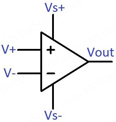
The input signals at inverting terminal results in opposite polarity output where as the inputs signals at non-inverting terminal produces same polarity output.
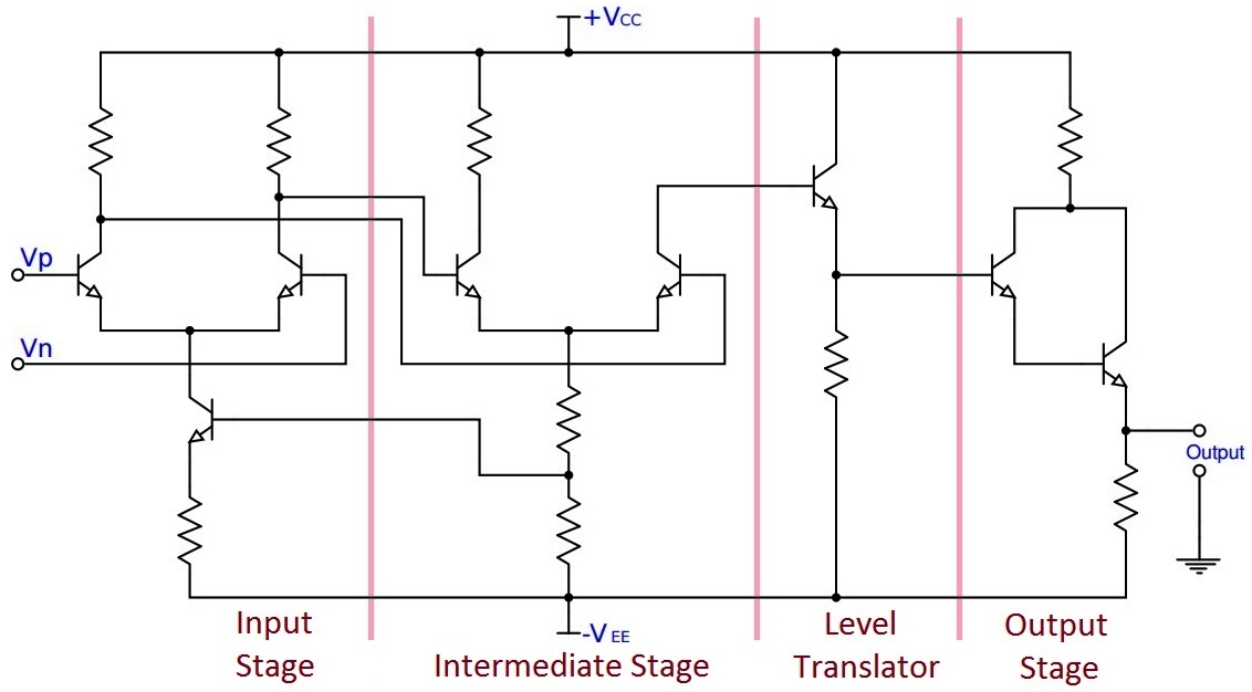
Block Diagram of an Opamp
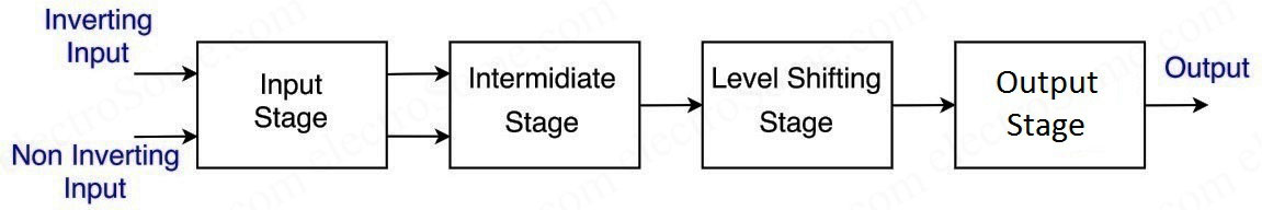
The Input Stage is a dual input balanced output differential amplifier which provides most of the voltage gain of amplifier and also establishes the input resistance of op-amp. Intermediate Stage is a dual input unbalanced output differential amplifier. DC voltage at the output stage will be above ground potential due to direct coupling. Therefore, a Level Shifting Stage is used to shift the dc level to zero. The Output Stage is usually a complementary push-pull amplifier which increases output voltage swing and current supplying capability of the op-amp. It also responsible for establishing low output resistance of the opamp.
Please read the article Differential Amplifier using Transistors for more information.
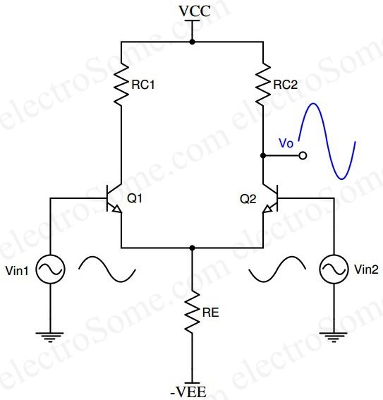
Input Stage
As explained above, Input Stage is a dual input balanced output differential amplifier which provides most of the voltage gain of amplifier and also establishes the input resistance of op-amp. Simple circuit of a dual input balanced output differential amplifier is shown below.

Intermediate Stage
As explained above, Intermediate Stage is a dual input unbalanced output differential amplifier. A simple circuit of a dual input unbalanced output differential amplifier is shown below.
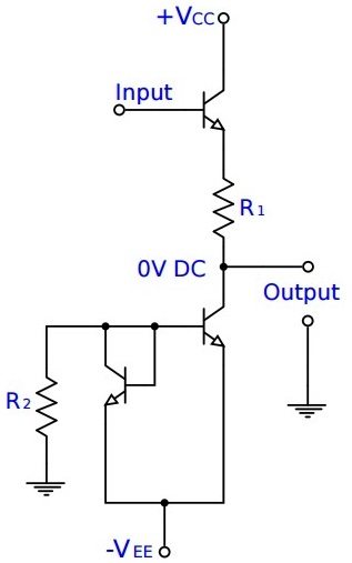
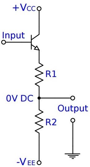
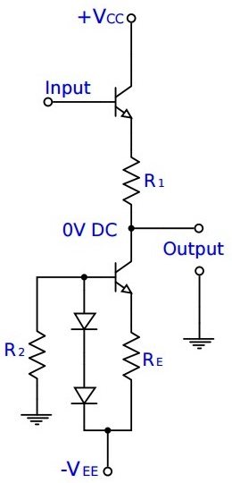
Level Shifting Stage
Since opamps are direct coupled, dc level at the output will be above zero. Each amplifier stage produces AC amplification of the signal but at the same time the DC level is shifted due to the bias voltages. So we need to use level translator circuits to shift dc level to zero. We can use voltage divider emitter follower for that purpose. DC voltage is determined by the ratio of R1 and R2. For better results we may also current mirror or diode current bias circuits as below.
Output Stage
This stage should be capable of supplying load current and should have low output resistance. Complementary push pull amplifier increases the output voltage swing of the output signal and also increases the current supplying capability of op-amp.
Simple Opamp Circuit Diagram
Opamp Characteristics
Ideal Opamp
An ideal opamp is a concept (not really exists) which enables us to state the characteristics of a perfect/ideal amplifier.
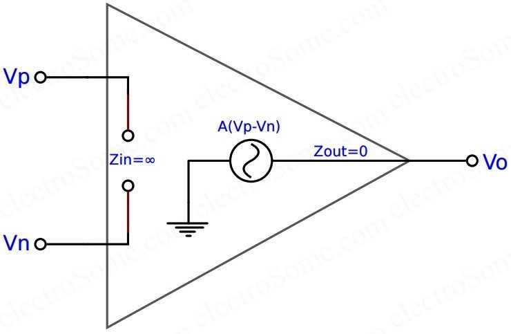
Characteristics of an Ideal Opamp
- Infinite open loop voltage gain
- Infinite input impedance
- Zero output impedance
- Infinite bandwidth
- Zero input offset voltage
- Zero common mode gain
- Infinite CMRR (Common Mode Rejection Ratio)
- Zero DC output offset
- Zero noise contribution
- Infinite power supply rejection ratio
- Positive and negative voltage swings to supply rail
- Output swings instantly to the correct value
Golden Rules of Opamp
These ideal characteristics of opamp can be summarized as two golden rules.
- In a closed loop circuit, opamp output will do whatever it can do to make the voltage difference between the inputs zero.
- Opamp inputs draws no current.
Real Opamp
Real vs Ideal Opamp
| Parameter | Ideal Opamp | Real Opamp |
|---|---|---|
| Voltage Gain | ∞ | 105 ~ 109 |
| Input Resistance | ∞ | 106Ω (BJT) 109 ~ 1012Ω (FET) |
| Output Resistance | 0 | 100 ~ 1000Ω |
| Common Mode Gain | 0 | 10-5 |
| Gain Bandwidth Product | ∞ | 1 ~ 20MHz |
Parameters of an Opamp
Input Offset Voltage
It is the voltage that must be applied between two input terminals to nullify the output. As shown in the figure below Vdc1, Vdc2 are dc input voltages and Vio is the input offset voltage.
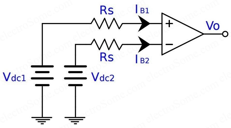
- Vio = Vdc1 – Vdc2
Higher the matching between input terminals, smaller the value of Vio . For 741 opamp, the maximum value of Vio is 6mV. Ideally opamp output will be zero when both input terminals are grounded.
Input Offset Current
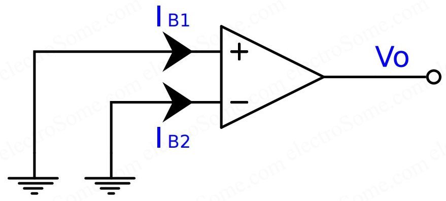
Input offset current is the algebraic difference between currents through two input terminals. Let IB1 be the current through non-inverting terminal and IB2 be the current through inverting terminal. Then the input offset current is given by,
- Iio=|IB1 – IB2|
Higher the matching between input terminals, smaller the value of Iio. For 741 opamp, the maximum value of Iio is 200nA.
Input Bias Current
It is the average value of currents through inverting and non-inverting terminals of an opamp.
- Input bias current, IB = (IB1 + IB2)/2
For 741 opamp, the maximum value of IB is 500nA.
Differential Input Resistance (Ri)
Differential Input Resistance is the equivalent resistance measured across either of input terminals with respect to ground.
For 741 opamp, differential input resistance value is relatively high in the order of 2MΩ.
Input Capacitance (Ci)
It is the capacitance measured across either of input terminals with respect to ground.
The value of Ci for 741 opamp is 1.4pF.
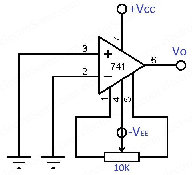
Offset Voltage Adjustment Range
Some opamps like UA741 or LM741 have offset null inputs (1st and 5th pin). These pins can be used to nullify the output when inputs are shorted. The range of output voltage which can be adjusted through this is called offset voltage adjustment range. Typically for 741 opamp it is ±15mV.
Input Voltage Range
Opamp will cease functioning properly if the voltage at either of input terminals exceeding this limit. For 741 opamp the limit is ±13V.
Common Mode Rejection Ratio (CMRR)
The ability to reject common mode signal is called Common Mode Rejection Ratio (CMRR). It can also be defined as the ratio of differential gain to common mode gain.
| CMRR | = |differential gain/common mode gain| |
| = |Ad/Ac| | |
|
CMRR |
Unit of CMRR is dB
= 20log|Ad/Ac| |
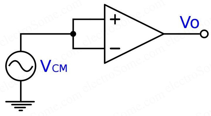
As mentioned earlier, ideally output will be zero in common mode which implies infinite CMRR.
CMRR is expressed in decibels (dB) and the typical value of CMRR of 741 opamp is 95dB.
Supply Voltage Rejection Ratio (SVRR)
SVRR is the ratio of change in op-amp’s input offset voltage to the change in supply voltage. It is also known as Power Supply Rejection Ratio (PSRR) or Power Supply Sensitivity (PSS). This can be expressed in microvolts/volts or decibels (dB).
- SVRR = ∆Vio/∆V
For 741 opamp SVRR is 150µV/V.
Output Voltage Swing
It is the maximum positive or negative output voltage that can be obtained without wave clipping. This will vary depending on the output load impedance and supply voltage.
Typical output voltage swing of 741 opamp is ±14V when the supply voltage is ±15V and load impedance is greater than 10KΩ.
Slew Rate (SR)
SR is defined as the maximum rate of change of output voltage per unit time. It is expressed in volts per microsecond.
- SR = dVo/dt V/µS
It indicates how rapidly the output of an op-amp changes in response to changes in input. Slew rate changes with voltage gain and is normally specified at unity gain. SR is a key factor for selecting opamp for AC applications.
Typical slew rate of 741 opamp is 0.5V/µS.
Gain – Bandwidth Product (GB)
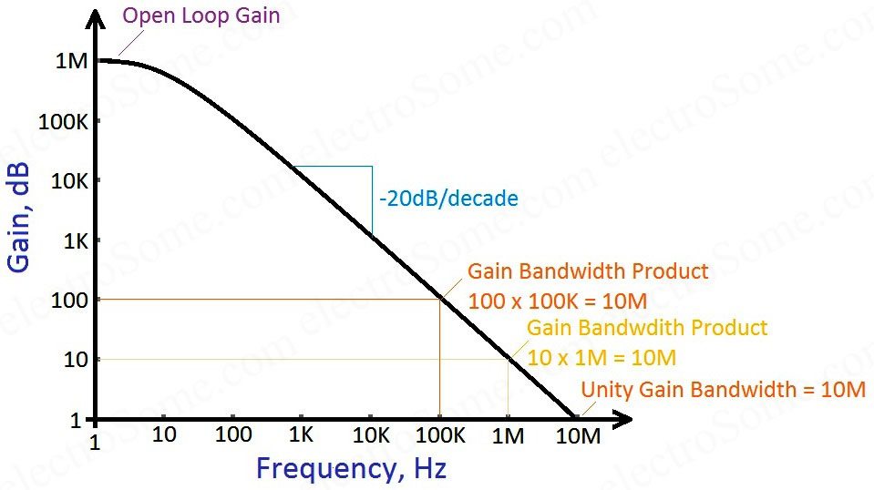
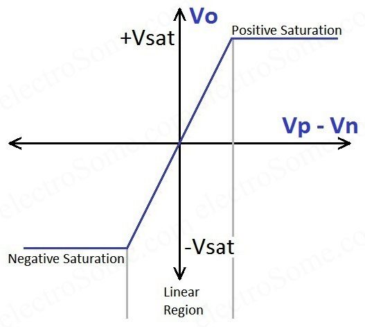
Gain Bandwidth Product describes op-amp’s gain in different frequencies. It is defined as the bandwidth of an opamp when voltage gain is one. As shown in the above graph, open loop gain falls at the rate of -20dB/decade. This means that if we double the frequency, gain drops by half. And if we half the frequency, gain doubles. This implies that product of gain and bandwidth are almost constant. That is the significance of Gain Bandwidth Product.
For 741 opamp, GB is approximately 1MHz.
Large Signal Voltage Gain
This is the gain of the opamp in DC, ie low frequency. It is usually quoted in V/mV.
- Voltage Gain = Output Voltage/Differential Input Voltage
- A = V/Vid
Typical large signal voltage gain of 741 opamp is 200V/mV.
Transient Response
Transient response gives us the information about how an opamp will work for a pulse input. Usually datasheets will specify rise time and overshoot. Rise time is the time taken by a signal to rise from 10% to 90% of its final value while overshoot is the occurrence of the signal exceeding its target.
Rise time of 741 opamp is 0.3μS and overshoot is 5%.
Output Short Circuit Current
Output short circuit current gives us the maximum current that can source or sink from the output of an opamp. In some applications opamp may needs to drive whose impedance is approximately zero (means output voltage approximately zero).
Output short circuit current of 741 opamp is 25mA.
Input Offset Voltage Drift
This indicates the change of input offset voltage with respect to temperature change. For 741 opamp it is 15μV/°C. So for a circuit to be operated in the range of 0 ~ 50°C, input offset voltage will change by 15μV/°C x 50°C = 0.75mV in the worst case scenario.
Supply Current
Current drawn by an opamp from the power supply with no load condition is termed as Supply Current. For 741 opamp, the maximum supply current is 2.8mA.
Operation
As we seen above an opamp have two inputs, non-inverting input (V+ or Vp) and inverting input (V- or Vn). Ideally it will amplify only the difference between those two inputs which is called as differential input voltage (Vp – Vn or V+ – V-).
- Vout = AOL(Vp – Vn)
Where AOL is the open loop gain of the opamp.
Open Loop Amplifier
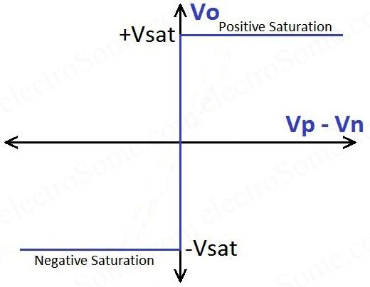
Open loop gain (AOL) is the gain of an op-amp when no feedback is given. Typically AOL is very high, for opamp ICs it is higher than 100,000. So even a very small difference in Vp and Vn will drive the output to supply voltage. The condition when the output voltage becomes greater than or equal to supply voltage is termed as saturation of the amplifier. Magnitude of open loop gain (AOL) is not properly controlled by the fabrication/manufacturing process and this very high gain may pick up a lot of noise. Due to these reasons it is impractical to use open loop configuration as a standard differential amplifier. So generally we will use open loop amplifier only as a comparator.
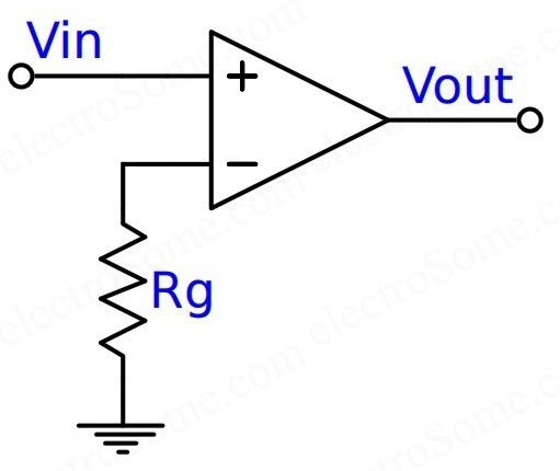
In the above circuit the inverting input Vn is held ground (0V) by a resistor Rg. So when the Vin is positive, Vout will be positive maximum and when the Vin is negative, Vout will be negative maximum.
Closed Loop
Closed loop amplifier can be made by providing a portion of output to the input. We can have negative feedback or positive feedback depending on the input (inverting or non-inverting) to which feedback is given.
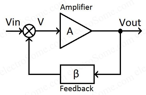
Where,
- A is the open loop gain
- β is the feedback factor
From the fig.
- V = Vin – Vout * β ——————(1) (negative feedback)
- Vout = A* V ——————(2)
Substituting (1) in (2) =>
- Vout = A(Vin – Vout * β)
- Vout= AVin – AVoutβ
- AVin = Vout + AVoutβ
- AVin = Vout(1 + Aβ)
- Vout/Vin = A/(1 + Aβ)
Thus,
- Negative Feedback Closed Loop Gain, Vout/Vin = A/(1 + Aβ)
- Positive Feedback Closed Loop Gain, Vout/Vin = A/(1 – Aβ)
Negative Feedback
Negative feedback is generally employed when the opamp is used as an amplifier. It makes the opamp operation predictable. When negative feedback is employed overall gain and circuit performance is mostly determined by the feedback network.

Advantages of Negative Feedback
- Reduces noise and distortion
- Improves stability
- Increases bandwidth
- Increases input impedance
- Reduces output impedance
- Reduces sensitivity to external changes
Positive Feedback
Comparators with hysteresis and oscillators generally employ positive feedback for its functionality.
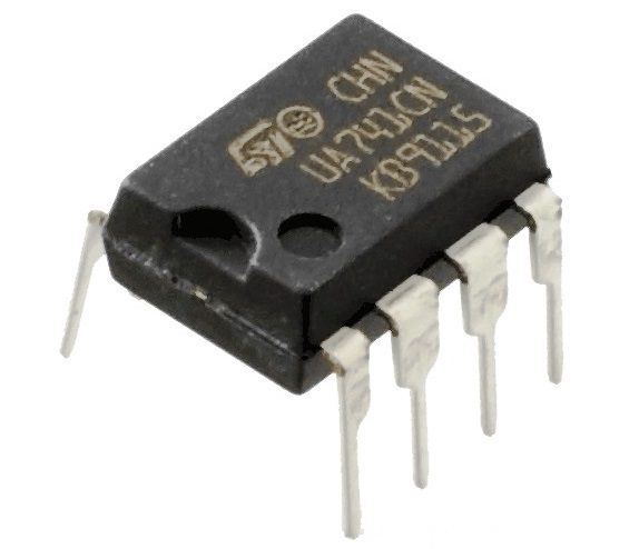
741 Opamp
LM741/UA741 is the most popular opamp IC and is designed by Dave Fullagar of Fairchild Semiconductor in 1968.
Pinout
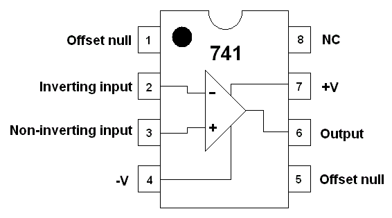
| No. | Name |
|---|---|
| 1 | Offset Null |
| 2 | Inverting Input |
| 3 | Non-inverting Input |
| 4 | -V |
| 5 | Offset Null |
| 6 | Output |
| 7 | +V |
| 8 | NC – No Connection |


Well documented with valuable details