Contents
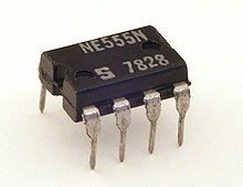
An Astable Multivibrator is an oscillator circuit that continuously produces rectangular wave without the aid of external triggering. So Astable Multivibrator is also known as Free Running Multivibrator. I have already posted about Astable Multivibrator using Transistors. Astable Multivibrator using 555 Timer is very simple, easy to design, very stable and low cost. It can be used for timing from microseconds to hours. Due to these reasons 555 has a large number of applications and it is a popular IC among electronics hobbyists.
Astable Multivibrator using 555 – Circuit
Above figure shows the circuit diagram of a 555 Timer wired in Astable Mode. 8th pin and 1st pin of the IC are used to give power, Vcc and GND respectively. The 4th pin is RESET pin which is active low and is connected to Vcc to avoid accidental resets. 5th pin is the Control Voltage pin which is not used. So to avoid high frequency noises it is connected to a capacitor C’ whose other end is connected to ground. Usually C’ = 0.01μF. The Trigger (pin 2) and Threshold (pin 6) inputs are connected to the capacitor which determines the output of the timer. Discharge pin (pin 7) is connected to the resistor Rb such that the capacitor can discharge through Rb. Diode D connected in parallel to Rb is only used when an output of duty cycle less than or equal to 50% is required. For the sake of explaing the working Circuit Diagram with Internal Block diagram is shown below.
Circuit with Internal Block Diagram
Since the Control Voltage (pin 5) is not used the comparator reference voltages will be 2/3 Vcc and 1/3 Vcc respectively. So the output of the 555 will set (goes high) when the capacitor voltage goes below 1/3 Vcc and output will reset (goes low) when the capacitor voltage goes above 2/3 Vcc.
Working
- When the circuit is switched ON, the capacitor (C) voltage will be less than 1/3 Vcc. So the output of the lower comparator will be HIGH and of the higher comparator will be LOW. This SETs the output of the SR Flip-flop.
- Thus the discharging transistor will be OFF and the capacitor C starts charging from Vcc through resistor Ra & Rb.
- When the capacitor voltage will become greater than 1/3 Vcc ( less than 2/3 Vcc ), the output of both comparators will be LOW and the output of SR Flip-flop will be same as the previous condition. Thus the capacitor continuous to charge.
- When the capacitor voltage will becomes slightly greater than 2/3 Vcc the output of the higher comparator will be HIGH and of lower comparator will be LOW. This resets the SR Flip-flop.
- Thus the discharging transistor turns ON and the capacitor starts discharging through resistor Rb.
- Soon the capacitor voltage will be less than 2/3 Vcc and output of both comparators will be LOW. So the output of the SR Flip-flop will be the previous state.
- So the discharging of capacitor continuous.
- When the capacitor voltage will become less than 1/3 Vcc, the output SETs since the output of lower comparator is HIGH and of higher comparator is LOW and the capacitor starts charging again.
- This process continuous and a rectangular wave will be obtained at the output.
Design
Capacitor Charges through Ra and Rb.
- Thigh = 0.693(Ra + Rb)C
Capacitor Discharges through Rb
- Tlow = 0.693RbC
- Output Frequency = 1/(Tlow + Thigh) = 1.44/((Ra + 2Rb) * C)
- Duty Cycle = Thigh/(Thigh + Tlow)
Where Thigh and Tlow are the time period of HIGH and LOW of the output of 555.
From this we can find that Duty Cycle less than or equal to 50% cannot be obtained. There are two ways to obtain this.
- Inverting the output
- Using a Diode Parallel to resistor Rb
Inverting the Output
In this method, just compliment the output. Thus the Duty Cycle = Tlow/(Tlow + Thigh). Where Tlow and Thigh are the time period of LOW and HIGH of output of 555. In this method the duty cycle of the output of 555 will be greater than 50% and that of inverter will be less than 50%.
Duty Cycle of 555 = 1 – Duty Cycle of Inverter
Using a Diode Parallel to resistor Rb
In this method we will connect a diode parallel to resistor Rb as shown dotted in the first circuit diagram above. Thus the charging current of capacitor will bypass the resistor Rb. Thus Thigh = 0.693RaC
Thus a Duty Cycle less than or equal to 50% can easily obtained.
Calculator
