
Contents
Pulse Width Modulation (PWM) is the one of the simple and most commonly used technique to produce analog voltages from digital signals. It has a wide variety of applications such as Digital to Analog Converter (DAC), DC Motor Speed Control, Sine Wave Inverters, Brightness control etc.
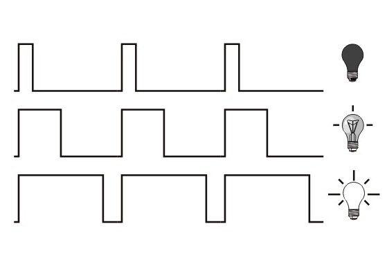
PWM signals are ON – OFF signals (HIGH or LOW) (hence the name Pulse) whose HIGH or ON duration is changed (hence Width Modulation) in accordance with our requirements. The fraction of time period for which the signal is ON to the total time period is termed as Duty Cycle.
PWM waves can be easily generated using CCP modules available with most of the PIC Microcontrollers. CCP stands for Capture / Compare / PWM, which means that it can be used for Capture or Compare or PWM operations. To program this module with MPLAB XC8 compiler we need to learn its working. Here for demonstration we are using PIC 16F877A microcontroller.
CCP – Capture / Compare / PWM Module
Microchip’s PIC 16F877A microcontroller has two CCP modules, named as CCP1 and CCP2. Each CCP module comprises of two 8 bit registers which can be operate as :
- 16 bit Capture Register
- 16 bit Compare Register
- PWM Master / Slave Duty Cycle register
This tutorial deals only with PWM operation of CCP module. Using this we can generate PWM output having resolution up to 10 bit. Output of CCP modules are multiplexed with RC1 & RC2 of PORTC, hence TRIS<1> and TRIS<2> must be cleared to make these pins output.
Working
The simplified block diagram of PWM mode of CCP module is shown below.
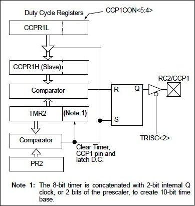
Timer 2 module provides the time base for the PWM operation of both CCP modules. The value of the TMR2 register increases from zero to maximum value as per the timer 2 input clock. The input clock is determined by the microcontroller clock frequency (Fosc) and timer 2 prescaler value.
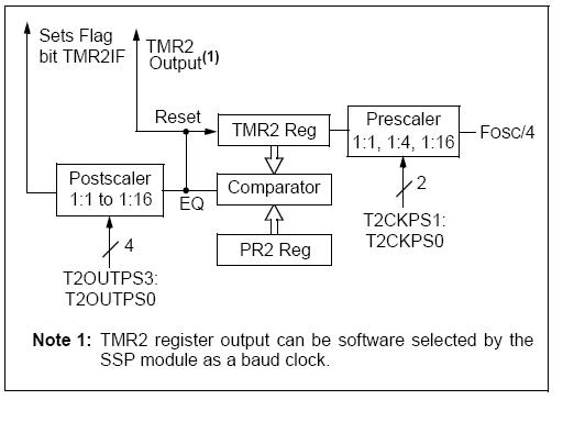
- Prescaler Input Clock : Fosc / 4
- Timer 2 Input Clock : (Fosc / 4) / Prescaler Value = Fosc / (4*Prescaler)
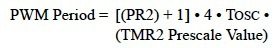
Time period of the generated PWM waves are determined by the value of PR2 Register. The comparator compares the values of PR2 and TMR2 registers. When these values become equal, the output pulse from the comparator sets the PWM output to HIGH. It also resets the Timer 2 value to zero.
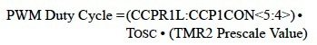
The PWM duty cycle is determined by the value in the CCPR1L and CCP1CON<5:4> registers, which can be written any time. This value is stored to CCPR1H and a 2 bit internal latch when there is a match between PR2 and Timer 2. This avoids the possibility of glitches in the PWM output due to changing of duty cycle.
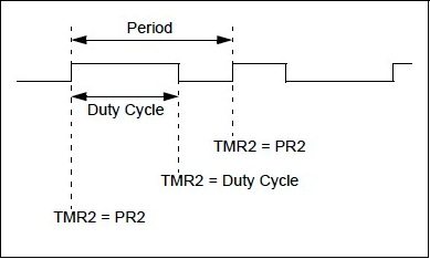
The PWM output become LOW when there is a match between Timer 2 value and Duty Cycle (CCPR1L and CCP1CON<5:4>).
Note 1 : The value of Duty Cycle should be less than Time Period (PR2) for the proper generation of PWM signals.
Note 2 : It is not possible to use different PWM frequencies for both CCP modules, because they use Timer 2 for their operation.
PWM Resolution
PWM Resolution of CCP modules can be calculated using the following equation.

Configuration
- Set the PWM Period by writing to PR2 register. The relation between PR2 value and time period is shown below.
- Then set the PWM Duty Cycle by writing to CCPR1L and CCP1CON<5:4> registers. The relation between register value and duty cycle is shown below.
- Configure the CCP pins as Output by writing to TRIS<2> and TRIS<1> bits.
- Set the Timer 2 (TMR2) prescale value and enable it by writing to T2CON register.
- Finally, configure the CCP module for PWM operation by writing to CCP control registers.
Circuit Diagram
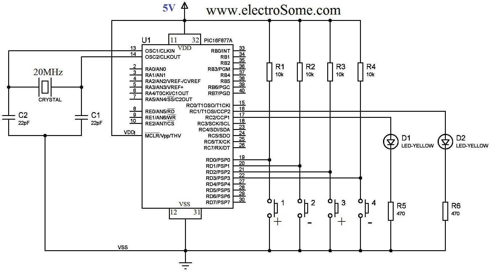
This circuit can be used to demonstrate the working of PWM. An LED is connected to the output of each CCP module through a series resistor to limit the current. Push Button Switches are used to adjust the PWM duty of both channels. We can see that the light intensity of LED increases as the PWM duty increases.
MPLAB XC8 Program
#define _XTAL_FREQ 20000000
#define TMR2PRESCALE 4

#include <xc.h>

// BEGIN CONFIG
#pragma config FOSC = HS   // Oscillator Selection bits (HS oscillator)
#pragma config WDTE = OFF  // Watchdog Timer Enable bit (WDT enabled)
#pragma config PWRTE = OFF // Power-up Timer Enable bit (PWRT disabled)
#pragma config BOREN = ON  // Brown-out Reset Enable bit (BOR enabled)
#pragma config LVP = OFF   // Low-Voltage (Single-Supply) In-Circuit Serial Programming Enable bit (RB3 is digital I/O, HV on MCLR must be used for programming)
#pragma config CPD = OFF   // Data EEPROM Memory Code Protection bit (Data EEPROM code protection off)
#pragma config WRT = OFF   // Flash Program Memory Write Enable bits (Write protection off; all program memory may be written to by EECON control)
#pragma config CP = OFF   // Flash Program Memory Code Protection bit (Code protection off)
//END CONFIG

long freq;

int PWM_Max_Duty()
{
  return(_XTAL_FREQ/(freq*TMR2PRESCALE);
}

PWM1_Init(long fre)
{
  PR2 = (_XTAL_FREQ/(fre*4*TMR2PRESCALE)) - 1;
  freq = fre;
}

PWM2_Init(long fre)
{
  PR2 = (_XTAL_FREQ/(fre*4*TMR2PRESCALE)) - 1;
  freq = fre;
}

PWM1_Duty(unsigned int duty)
{
  if(duty<1024)
  {
    duty = ((float)duty/1023)*PWM_Max_Duty();
    CCP1X = duty & 2;
    CCP1Y = duty & 1;
    CCPR1L = duty>>2;
  }
}

PWM2_Duty(unsigned int duty)
{
  if(duty<1024)
  {
    duty = ((float)duty/1023)*PWM_Max_Duty();
    CCP2X = duty & 2;
    CCP2Y = duty & 1;
    CCPR2L = duty>>2;
  }
}

PWM1_Start()
{
  CCP1M3 = 1;
  CCP1M2 = 1;
  #if TMR2PRESCALAR == 1
    T2CKPS0 = 0;
    T2CKPS1 = 0;
  #elif TMR2PRESCALAR == 4
    T2CKPS0 = 1;
    T2CKPS1 = 0;
  #elif TMR2PRESCALAR == 16
    T2CKPS0 = 1;
    T2CKPS1 = 1;
  #endif
  TMR2ON = 1;
  TRISC2 = 0;
}

PWM1_Stop()
{
  CCP1M3 = 0;
  CCP1M2 = 0;
}

PWM2_Start()
{
  CCP2M3 = 1;
  CCP2M2 = 1;
  #if TMR2PRESCALE == 1
    T2CKPS0 = 0;
    T2CKPS1 = 0;
  #elif TMR2PRESCALE == 4
    T2CKPS0 = 1;
    T2CKPS1 = 0;
  #elif TMR2PRESCALE == 16
    T2CKPS0 = 1;
    T2CKPS1 = 1;
  #endif
    TMR2ON = 1;
    TRISC1 = 0;
}

PWM2_Stop()
{
  CCP2M3 = 0;
  CCP2M2 = 0;
}

void main()
{
  unsigned int i=0,j=0;
  PWM1_Init(5000);
  PWM2_Init(5000);
  TRISD = 0xFF;
  TRISB = 0;
  PWM1_Duty(0);
  PWM2_Duty(0);
  PWM1_Start();
  PWM2_Start();
  do
  {
    if(RD0 == 0 && i<1000)
      i=i+10;
    if(RD1 == 0 && i>0)
      i=i-10;
    if(RD2 == 0 && j<1000)
      j=j+10;
    if(RD3 == 0 && j>0)
      j=j-10;
    PWM1_Duty(i);
    PWM2_Duty(j);

    __delay_ms(50);
  }while(1);
}
- PWM1_Init(frequency) & PWM2_Init(frequency) will initialize the CCP1 and CCP2 modules respectively in the PWM mode with the specified frequency. You can’t have different frequencies for CCP modules as both of them uses Timer 2 for their operation.
- PWM1_Duty(duty) & PWM2_Duty(duty) will set the duty cycle of the generated PWM signals. The parameter duty can be any value ranging from 0 to 1023 corresponding to 0% to 100% duty cycle.
- PWM1_Start() & PWM2_Start() are used to initialize / start the PWM signal generation.
- PWM1_Stop() & PWM2_Stop() are used to stop the PWM signal generation.
Download Here
You can download MPLAB XC8 project files here.
Video
