

Getting Started with DipTrace
DipTrace is a software that allows you to create simple and complex Printed Circuit Boards from schematic diagrams to layouts. It is a user friendly EDA software. We recommend this for electronics hobbyists, as it is a freeware allows us to design single layer and double layer PCBs upto 300 pins. You can purchase its paid version if you need more layers/pins.
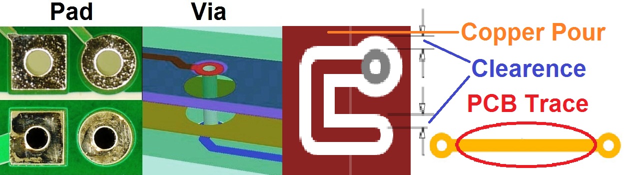
If you are a beginner to PCB designing, you should be familiar with following terms before going to pcb designing.
- Symbol
- Footprint or Pattern
- 3D Model
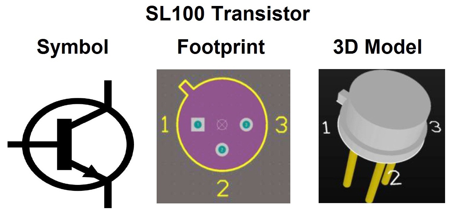
And the following image will help you to understand some commonly used PCB terms.
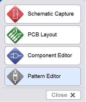
DipTrace consists of 4 sections :
- Schematic Capture
- PCB Layout
- Component Editor
- Pattern Editor
In these Component Editor and Pattern Editor allows us to create new components. Component Editor is for defining Symbol while Pattern Editor is for creating its Footprint. Circuit Diagrams can be drawn in Schematic Capture. After completing the circuit diagrams, these are converted into PCB by using PCB Layout. The PCB Layout enables us to manually / automatically place components and route conductive tracks.
Getting Started with DipTrace
In this section we will start learning DipTrace by designing a small trial PCB.
- Download DipTrace
- Install the Software
- Open Diptrace Launcher from Start Menu
- Select Schematic Capture from the Launcher
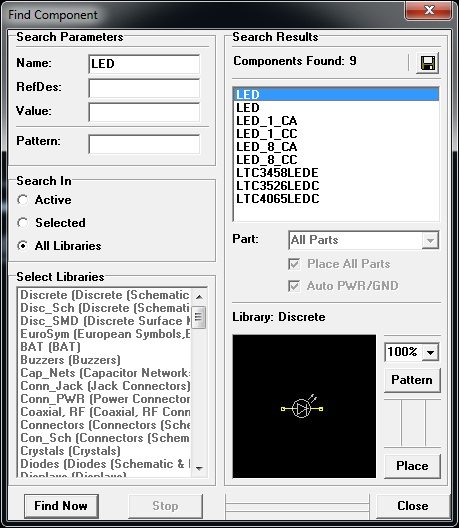
- You can use the Find Component tool in the Objects menu for finding and placing components.

- Make sure that Pattern (Footprint) is linked with the component you are using by clicking on the Pattern button.
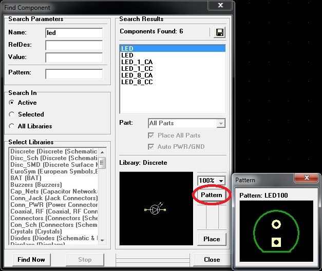
- Then click the Place button to add that component to Worksheet.
- You can also place the component from a particular library as follows. Here also you should make sure that Pattern / Footprint is linked with the component at the bottom left column. PJ-002A is the part number of a DC Jack.
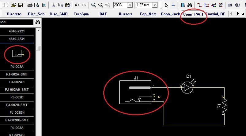
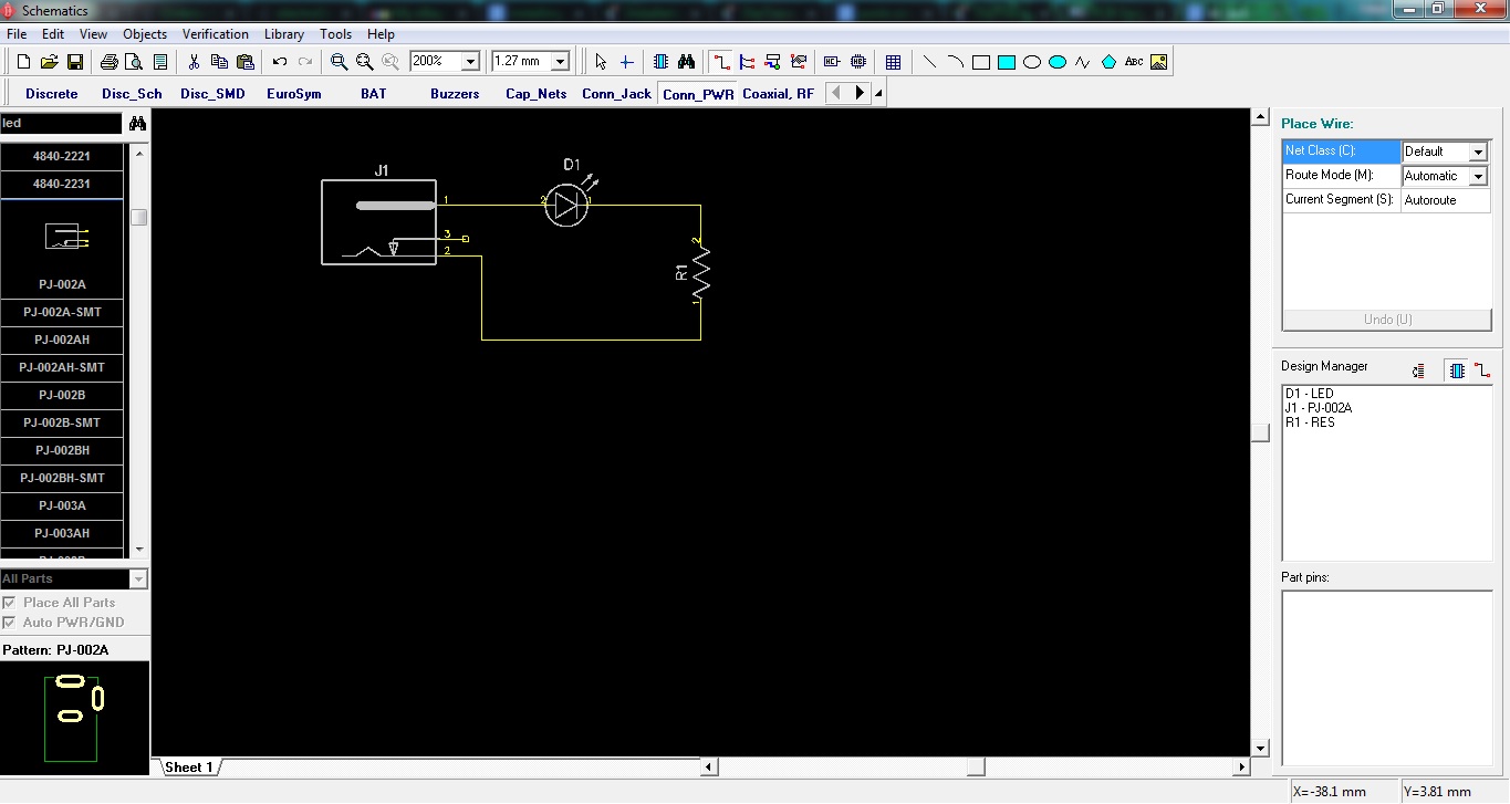
- Wire the simple circuit to glow an LED.

- After drawing the circuit, Save the Schematic.
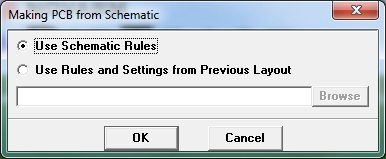
- Then import it to PCB Layout by pressing Ctrl+B or select File >> Convert to PCB
- Click Ok for the dialog box appeared.

- Arrange the components so that they occupy minimum space.
- You can adjust the Solder Pad sizes such that you can properly solder it. Right Click on Pad >> Pad Properties

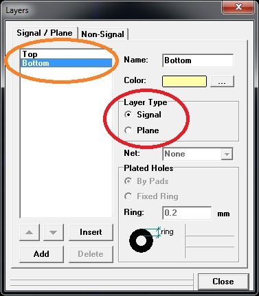
- Here we need only Single Sided PCB (Copper conductive track on one side and Components on the other side). Go to Route option in menu bar and select Layer Setup. Mark Bottom Layer as Signal and Top as Plane.
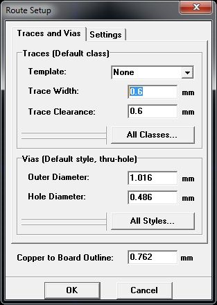
- To set conductive trace width and trace clearance, go to Route >> Route Setup.
- To autoroute the PCB click Route >> Run Autorouter.
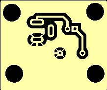
- After Routing is complete, top view and bottom view.


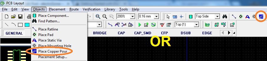
- Next step is to add Copper Pour to PCB. Copper Pour reduces noises, makes etching easy and provide strength to PCB. Firstly Select Bottom Layer as given above.
- Open the Copper Pour Tool.
- Then draw border of the PCB around the components and press enter after completing.
- Select Net Clearance as 1mm. In the connectivity option, select the net (Usually Ground net) in the Connect to Net and Thermals as 4 spoke. (Net name of a particular Pad or Trace can be find by right clicking on it).
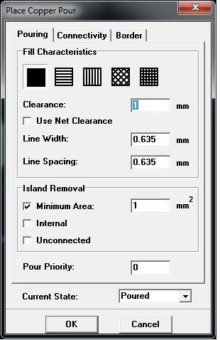
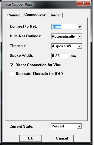
- Click Ok
- Next step is to add Mounting Hole, for that select Objects >> Place Mounting Hole. Place mounting hole in each corner of the PCB design and you can edit it dimensions by right clicking on it. (Generally 6mm outer diameter and 4mm inner diameter).
- Now update the copper pour. Right Click on Copper pour border >> Update
- Finally

Now you can export or print your PCBs using the options given the File Menu. Hope this tutorial will give you a quick start on DipTrace. We will post more tutorials soon, stay tuned with us.
