

PCB Manufacturing Simplified by JLCPCB
During the beginning of my electronics engineering journey I used to make PCBs at home using toner transfer method. Later I used to do screen printing and also manufacture PCBs locally. Then I used to assemble components myself. In all these methods PCB manufacturing itself is a time consuming process. Sometimes some components won’t be readily available in the market which will further take more time to arrange.
Recently I have come across JLCPCB, which is a sister organization of EasyEDA which I have introduced you before. So in this article I would like to share my mind-blowing experience with JLCPCB with you.
I was planning to do a home automation project when I come across JLCPCB. They provide PCB manufacturing, SMT assembly, manual through hole assembly at a nominal price. So I decided to try it.
As usual first we need to select components required for this project. Here it was pretty easy as JLCPCB provide a component library with all details.

And the most easiest part is that footprint of these components are available in EasyEDA as shown below. Just search and add it with the part number you get from JLCPCB.

Thus I was able to quickly add all the required components and completed the schematics and PCB design. I have already written a tutorial about PCB designing with EasyEDA.


Once the PCB design is completed, we can directly place the order of PCB using menu “Fabrication >> PCB Fabrication File (Gerber).

Here it will show the option to download gerber files or directly order PCB at JLCPCB. Just click “Order PCB/SMT at JLCPCB”.

This will redirect to JLCPCB and it will provide you options to select various parameters for PCB manufacturing as shown below.


You can enable the option for SMT Assembly if you want JLCPCB to assemble your components. Then click confirm.

Next it will ask you to upload BOM and Pick & Place Files as shown below. These files can be downloaded from Fabrication menu in EasyEDA.

Sometimes some components of your BOM may out of stock. JLCPCB provides an option to select alternate components in these situations as shown below.

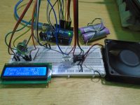
Once the inventory is selected properly you can click “Next”. This will give you the quote for the PCB order. Then you can simply place the order and get your PCB delivered in a week or two. See the images of the PCBs of my order below.


The PCB quality is very good and it was assembled properly. It was really good experience to use JLCPCB and I will be using it for my future projects.
Discount for New Users
After seeing this article JLCPCB has offered an $18 coupon for those who sign up using below link.