

Differential Amplifier using Transistors
Contents
As the name indicates Differential Amplifier is a dc-coupled amplifier that amplifies the difference between two input signals. It is the building block of analog integrated circuits and operational amplifiers (op-amp). One of the important feature of differential amplifier is that it tends to reject or nullify the part of input signals which is common to both inputs. This provides very good noise immunity in a lot of applications. Let’s see the block diagram of a differential amplifier.
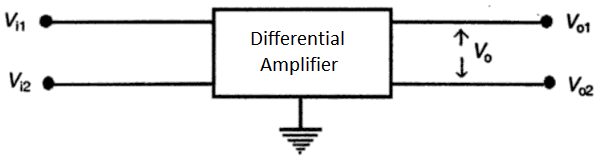
Vi1 and Vi2 are input terminals and Vo1 and Vo2 are output terminals with respect to ground. We can feed two input signals at the same time or one at a time. In the former case it is called dual input otherwise it is single input. Similarly there are two ways to take output also. If the output is taken from one terminal with respect to ground, it is unbalanced output or if the output is taken between two output terminals, it is balanced output.
Differential Amplifier using BJT
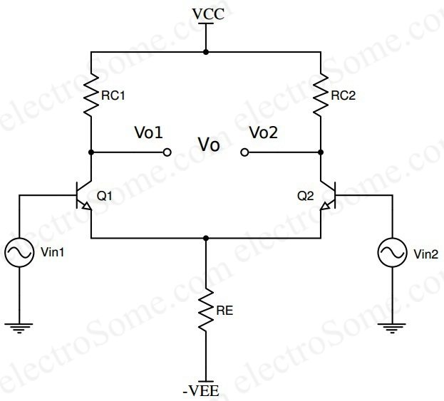
The simplest form of differential amplifier can be constructed using Bipolar Junction Transistors as shown in the below circuit diagram. It is constructed using two matching transistors in common emitter configuration whose emitters are tied together.
Configurations
Based on the methods of providing input and taking output, differential amplifiers can have four different configurations as below.
- Single Input Unbalanced Output
- Single Input Balanced Output
- Dual Input Unbalanced Output
- Dual Input Balanced Output
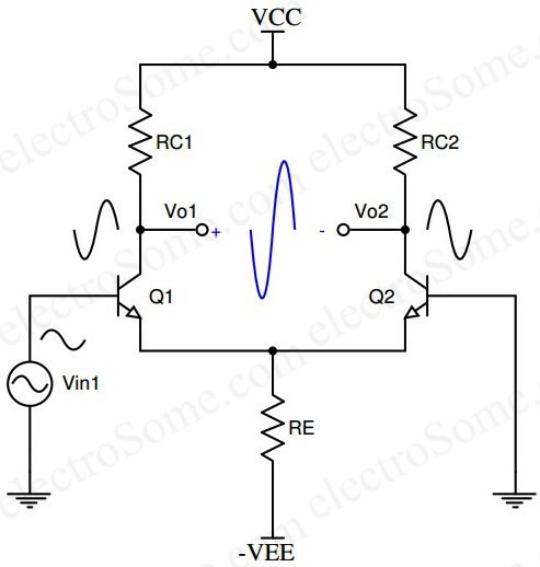
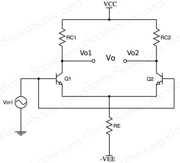
Single Input Unbalanced Output
In this case, only one input signal is given and the output is taken from only one of the two collectors with respect to ground as shown below.
When input signal Vin1 is applied to the transistor Q1, it’s amplified and inverted voltage gets generated at the collector of the transistor Q1. At the same time it’s amplified and non-inverted voltage gets generated at the collector of the transistor Q2 as shown in the above diagram. Unbalanced output will contain unnecessary dc content as it is a dc coupled amplifier therefore this configuration should follow by a level translator circuit.
How the transistor Q2 also producing output voltage even though the input is provided only to transistor Q1 ?
The effect of input voltage Vin1 is coupled to the transistor Q2 via the common emitter resistor RE. You can see the proof of this in the AC Analysis section.
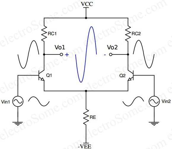
Single Input Balanced Output
As above only one input signal is given even though the output is taken from both collectors.
This will give us more amplified version of output as it is combining the effect of both transistors. There won’t be any unnecessary dc content in balanced output as the dc contents in both outputs gets canceled each other.
- Vo = Vo1 – Vo2
Dual Input Unbalanced Output
Both inputs are given in this case ie, differential input but the output is taken from only one of the two collectors with respect to ground as shown below.
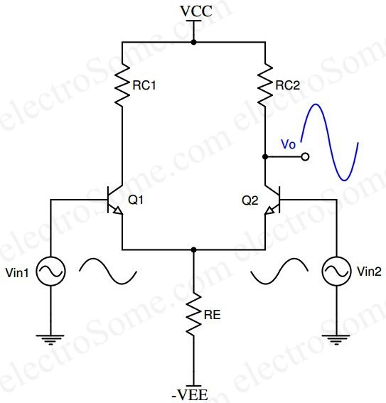
Amplified version of difference in both signals will be available at the output. The voltage gain is half the gain of the dual input, balanced output differential amplifier. Unbalanced output will contain unnecessary dc content as it is a dc coupled amplifier therefore this configuration should follow by a level translator circuit.
Dual Input Balanced Output
Above circuit consists of two identical transistors Q1 and Q2 with its emitters coupled together. Collectors are connected to main supply VCC through collector resistor Rc. Magnitude of power supplies VCC and –VEE will be same.
- Vo = Ad(Vin1 – Vin2)
Where Ad = differential gain
Vin1, Vin2 = input voltages
When Vin1 = Vin2, obviously the output will be zero. ie, differential amplifier suppresses common mode signals.
For effective operation, components on either sides should be match properly. Input signals are applied at base of each transistor and output is taken from both collector terminals. There won’t be any unnecessary dc content in balanced output as the dc contents in both outputs gets canceled each other.
DC Analysis
DC analysis provides the operating point values ICQ and VCEQ for the transistors used in the circuit. The DC equivalent circuit obtained by reducing all AC signals to zero as shown in figure below.

Assume :
- Source Resistance, RS1 = RS2 = RS
- Q1 = Q2
- RE1 = RE2 hence RE = RE1||RE2
- RC1 = RC2 = RC
- |VCC|=|VEE|
Applying KVL to base – emitter loop of Q1,
- -IBRS – VBE – 2IERE + VEE = 0 ———————-(1)
Since IC = βIB and IC ≈ IE
- IB ≈ IE/β ———————-(2)
Substituting (2) in (1) =>
- – IERS/β – VBE – 2IERE + VEE = 0
- – IE(RS/β – 2RE) + VEE – VBE = 0
Where VBE = 0.7V for silicon and 0.2V for germanium.
Also RS/β << 2RE
Therefore,
- IE = (VEE – VBE)/2RE ————————(3)
Eqn.(3) =>
- RE determines the emitter current of Q1 and Q2
- IE is independent of RC
Since the voltage drop across RS is too small, we can neglect it. So,
- VE = –VBE
- VC = VCC – ICRC
| VCE | = VC – VE |
| = (VCC – ICRC) – (–VBE) | |
| = VCC + VBE – ICRC ——————-(4) |
We can determine operating point values using equations (3) and (4). Since two transistors are identical, same equations can be used for both.
- IE = IC = (VEE – VBE)/2RE
- VCE = VCC + VBE – ICRC
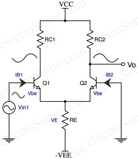
AC Analysis
We can find Voltage Gain Ad and Input Resistance Ri of the differential amplifier by doing AC Analysis. The ac equivalent circuit is obtained by reducing all DC voltage sources to zero and replacing transistor with its equivalent.

Since both dc emitter currents are equal resistances re1’ = re2’ = re’
Applying KVL in loop 1 and 2,
- Vin1 = RS1ib1 + ie1re’ + (ie1 + ie2)RE
- Vin2 = RS2ib2 + ie2re’ + (ie1 + ie2)RE
We know that,
ib1 ≈ ie1/β and ib2 ≈ ie2/β
Thus,
- Vin1 = (RS1/β) ie1 + ie1re’ + (ie1 + ie2) RE
- Vin2 = (RS2/β )ie2 + ie2re’ + (ie1 + ie2)RE
Consider RS1/ β & RS2/ β << RE & re’
- Vin1 = ie1 (re’ + RE) + ie2 RE
- Vin2 = ie2 (re’ + RE) + ie1RE
On solving these equations we get,
- ie1 = (Vin1(re’ + RE) – Vin2RE )/((re’ + RE)² – RE²) ———————(5)
- ie2 = (Vin2(re’ + RE) – Vin1RE)/ ((re’ + RE)² – RE² ) ———————(6)
Voltage Gain
| Output voltage, Vo | = VC2 – VC1 |
| = -RCic2 – (-RCic1) = Rc(ic1 – ic2) => Rc(ie1 – ie2) —————–(7) |
On substituting (5) and (6) in (7) and solving
Vo = (Rc(Vin1 -Vin2)(re’ – 2RE) )/(re’(re’ + 2RE))
Vo = (RC/re’)(Vin1 – Vin2) ——————————–(8)
Thus the differential gain, Ad = RC/re’
This proves a differential amplifier amplifies the difference between two input signals.
Differential Input Resistance
Differential Input Resistance is the equivalent resistance measured across either of input terminals and ground. Thus to find out Ri1, Vin2 should be grounded and to measure Ri2, Vin1 should be grounded.
| Ri1 | = Vin1/ib1 when Vin2 = 0 |
| = Vin1/(ie1/β) |
Substituting equation (5) of ie1
| Ri1 | = (Vin1β)/((Vin1(re’ + RE) – Vin2RE )/((re’ + RE)² – RE²)) |
| = β/((re‘ + RE)/(re‘2 + 2re‘RE) | |
| = βre‘(re‘ + 2RE)/(re‘ + RE) | |
| RE >> re‘ re‘ + 2RE ≈ 2RE re‘ + RE ≈ RE |
|
| Ri1 | = 2βre‘ |
- Ri1 = 2βre‘
Similarly,
- Ri2 = 2βre‘
Output resistance
The effective resistance measured at output terminal with respect to ground. So the output resistance is measured between the collector and the ground, which is same as the collector resistance RC.
- RO1 = RO2 = RC
Common Mode Rejection Ratio (CMRR)
Dual input balanced output differential amplifier should suppress the common signals present at its inputs. A differential amplifier is said to be in common mode when same signal is applied to both inputs and the expected output will be zero, ie ideally common mode gain is zero.
Effectiveness of rejection depends on the matching of two common – emitter stages used. The ability of a differential amplifier to reject common mode signal is called Common Mode Rejection Ratio (CMRR).
| CMRR | =|differential gain/common mode gain| |
| =|Ad/Ac| | |
|
CMRR |
Unit of CMRR is dB
= 20log|Ad/Ac| |
As mentioned earlier, ideally output will be zero in common mode which implies infinite CMRR.

Thank you so much
Please insert typical values for re of small signal transistors like 2N3904 or 2N2222 to get a practical value for gain.