

PCB Designing using OrCad Layout 10.5
Contents
OrCad is a highly developed and complex software that provides affordable and high performance PCB designing tools for small and industrial PCB designers. But for an electronic hobbyist, OrCad may seems to be highly complicated and time consuming when compared to other PCB designing tools. OrCad 9.2 is the commonly used version but it is not compatible with 64 bit and the next best choice is OrCad 10.5 as higher versions of OrCad are highly complicated.
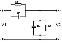
Thus in this tutorial, we will show how to design a simple Single Side PCB using OrCad Layout 10.5. One of the main problem that we may face is the difficulty to find footprints of different components. Here we solves this problem by creating a new library file which include commonly used footprints for an electronic hobbyist. You can download this library at the bottom of this article.
The first step in using Layout is the selection of Technology File. This file indicates the technology of the PCB that you are going to design. The installation will include different technology files for General Purpose, PCB with Jumper, Surface Mount devices etc… In this example tutorial we will use the technology file default.tch. If your circuit has too many connections and single side pcb is required then you should choose jumpxxxx.tch. This technology will automatically place jumpers during PCB routing.
Here is a video tutorial for you…
Steps :
- Open OrCad Layout 10.5
- File >> New
- Select the Technology File (*.tch) and MAX (*.max) file and click on Apply ECO
- Click on Cancel, if it asks for Netlist
- Use Zoom options to get a free area to draw circuit
- Right Click >> New >> Select Footprint and Add library, electroSome.llb
- Add the required components
- Place the required components on the workspace
- Adjust the Place Grid to a low value from Options >> System Settings, to place components more flexibly
- Select the Connection Tool, on the toolbar to wire up the circuit.
- After completing the circuit, goto Tool >> Layer >> Select From Spreadsheet, to set the PCB as Single Layer
- To set the track width of each connection, goto Tool >> Net >> Select From Spreadsheet
- Then draw a border for PCB by using Obstacle Tool on the toolbar
- Then for autorouting goto, Auto >> Autoroute >> Board
- Save your design using Save As
- Your PCB will be ready for printing now.
Now you can print the required layer ( bottom) or create a Gerber file using Post Processing. For this goto Options >> Post Process Settings and select the required layer. Then select the required option and close the spreadsheet. Then click on Auto >> Run Post Processor. Then the required file or print will be generated according to the selected options.
Tips :
- To Rotate a Component press R
- To Copy a Component press Ctrl + C
- To End Command press Esc
Library File :
You can download the library file, electroSome.llb here…
electroSome

