

EasyEDA – A Cloud based PCB Design Software
Contents
Cloud computing is an internet based computing which relies on sharing computer resources. It enables us to use computer resources or processing power as a utility similar to using electricity. So we don’t need to make big computer infrastructure in our building, just use the cloud resources whenever there is a need. Nowadays everything become cloud computing, like cloud storage, word processing, business analytics etc.
What is the role of cloud computing in electronics ? The question ends here, EasyEDA. It is a cloud based online circuit design, simulation and pcb design tool.
Advantages
Using EasyEDA has following advantages compared to other traditional tools like OrCad, Altium, DipTrace etc.
- No need to install any special softwares, a web browser is enough.
- Will work on all operating systems which supports a modern browser.
- Work on the go. You can work anywhere, any PC or even in mobile devices by just connecting to internet.
- No need of large resources or high power computers to do big projects.
- Access to large and updated libraries on the cloud which is created by a large user base
- No need to update the software, it is automatically applied to all clients when the server software is updated.
- Share your design with online community.
- Get and redesign designs from the community
Disadvantage
- Needs internet connection for its operation.
But it will work in offline mode once the tool is loaded in the browser and it can save the design locally. We can also hope that they will develop an offline tool or software for this purpose soon.
About Website
Their website https://easyeda.com/ is designed with best technologies available today. It is using SSL (Secure Socket Layer) HTTPS to secure the communication between user and the server. Its front is a responsive HTML5 design with SVG (Scalable Vector Graphics), Canvas, Web Socket, Web Worker, offline cache etc. And the backend is built with Nginx and PHP. Usage of Nginx ensures us faster response even when using SSL encryption.
My Review
In my point of view, they can provide a very good service to electronics engineers. I hope they can provide a low cost solution as their complete solution is made with open source softwares or technologies. And we can make or modify our designs in any devices which will supports a modern internet browser. In the user’s point of view there may be a lot of concerns to shift to EasyEDA. But they clearly answers all these concerns here : EasyEDA FAQ.
Getting Started
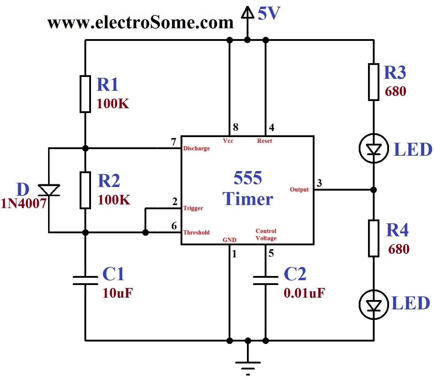
For the testing and demonstration we will make a Dancing Light using 555 Timer, circuit diagram is shown below.
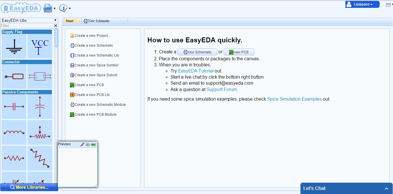
- Open the website https://easyeda.com
- Then register or login. You can also use Google or QQ Login
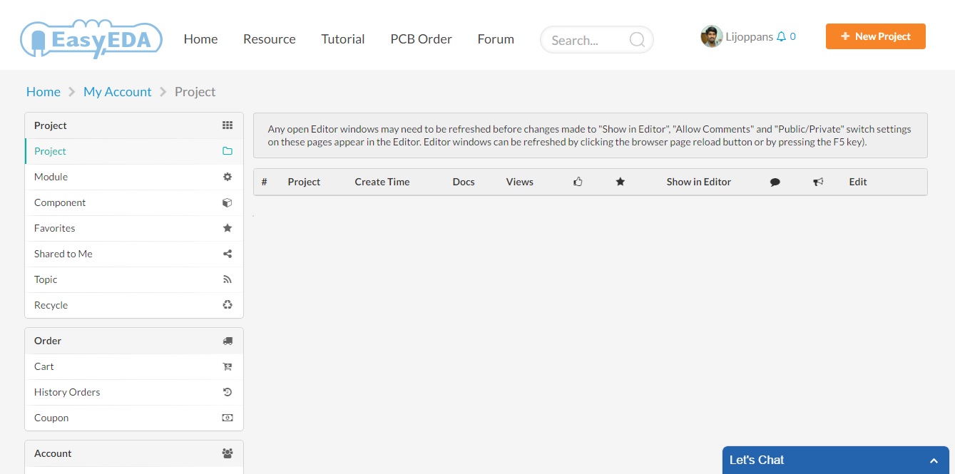
- After login, you will get redirected to accounts page. There you can manage all your projects, components, personal settings, orders etc.
My main concentration is on the EDA functionality, so I am directly going to start a project.
- New Project
As in a full fledged EDA tool, here also we can see a lot of options to start a project like Create a new Project, Create a new Schematic, Create a new Schematic Lib, Create a new Spice Symbol, Create a new Spice Subckt, Create a new PCB, Create a new PCB Lib, Create a new Schematic Module and Create a new PCB Module. In this tutorial we will create a new schematic, simulate and will make a pcb design for it.
- Create a New Schematic
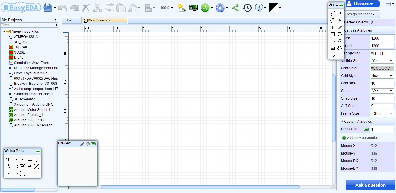
You can see that the complete UI (user interface) looks similar to an EDA software installed in our PC. You should make use of the filter tool in the top left corner which can be used to search components in the cloud database.
- Search and place 555 timer IC. Don’t forget to change the search section to EasyEDA Libs.
- For placing a component, just click (not dragging) once on it and move the cursor to the schematic editor.
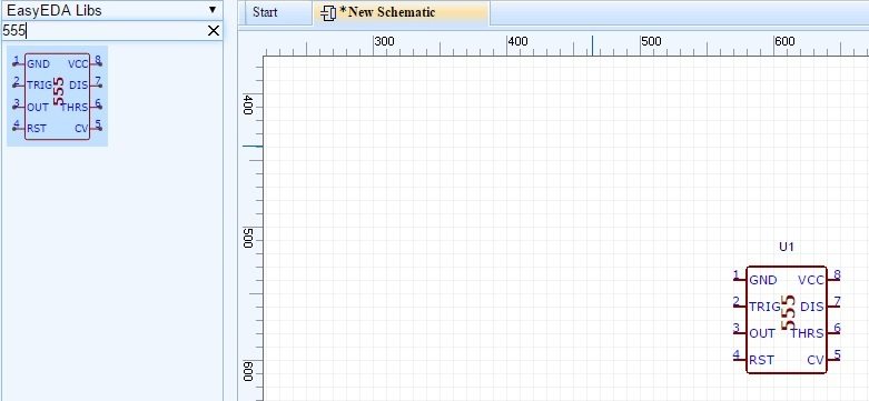
- You can clear the filter and place the rest of the components.
- As in other EDA tools, you can press “R” or space for rotating a component.
- Visit this URL of other shortcuts : https://easyeda.com/Doc/Tutorial/introduction.htm#Hotkeys
- For changing a component value, just select the component and edit it using Design Manager in the right side.
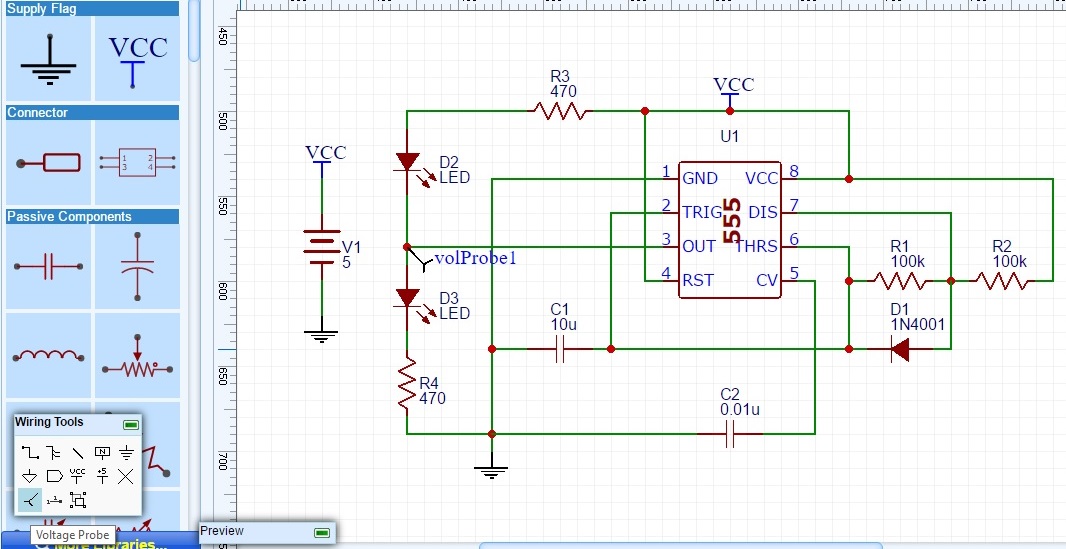
- Don’t forget to place Voltage Probe in the Wiring Tools at the output of 555 for spice simulation.
- Now, run the simulation

- Set the transient parameters, as per the output frequency of 555 timer.

- Run
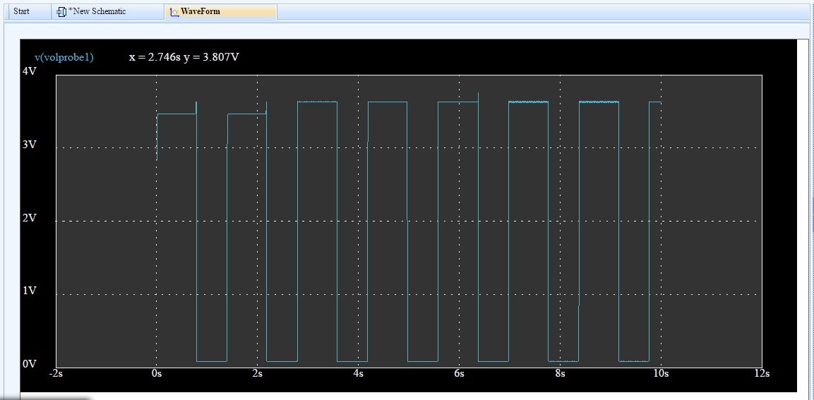
- So, the circuit is working fine.
- Go to Schematic again to make the PCB design.
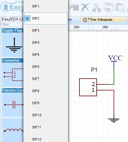
- We can place a 2 pin connector instead of battery in the PCB.
- Click on the Convert to PCB button.
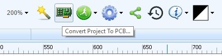
- It will automatic import components and connections to the PCB design tool of EasyEDA.
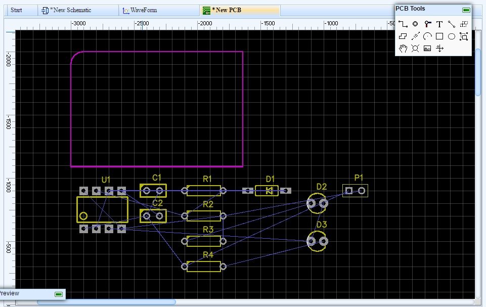
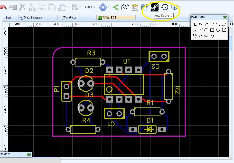
- Arrange the components inside the Board Outline and click autorouter.
- Note : It may take some time to complete the autorouting as it is done in a cloud computer and then loaded into the browser.
- Now add holes for PCB mounting.

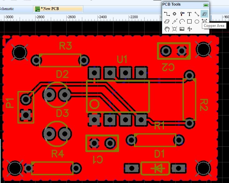
- Now add copper pour to both top and bottom layers using the Copper Area tool.
- Click on the Copper Area tool and draw border around the PCB.
- Add copper pour to the next layer by changing the active layer using the Layers tool in the bottom right corner.
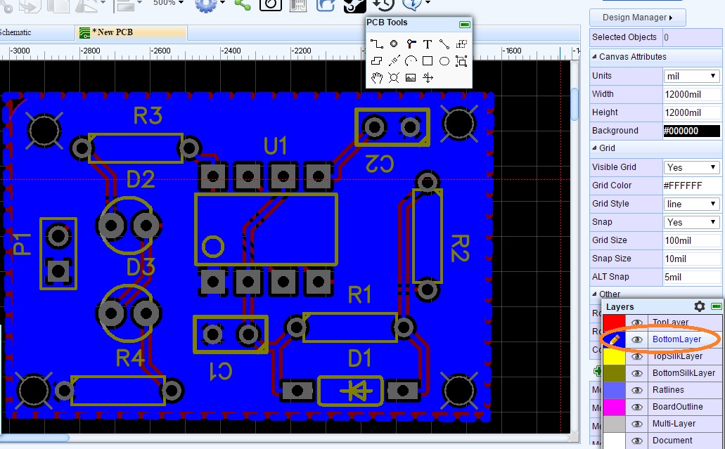
So the PCB design is completed. Now you may order sample PCBs online via EasyEDA or you can export the files.
Note : I just covered the basics only. Capabilities of EasyEDA is outside the scope of this article. You can go through official EasyEDA Tutorials for more details.


