

EasyEDA vs DipTrace vs OrCad
Contents
Today I am gonna write about my PCB designing journey that happened before 8 year. I started doing hobby circuits before 8 years and now I am doing professional circuits.
Phase 1 : Hand Drawn (no Software)
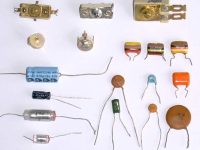
I started designing PCB manually without using any softwares. Mostly I used graph papers to design PCB as it was very easy to make measurements and alignments. Several iterations of drawing was required to make even a small circuit. After the design is completed, I used to copy the design to copper clad using permanent marker.
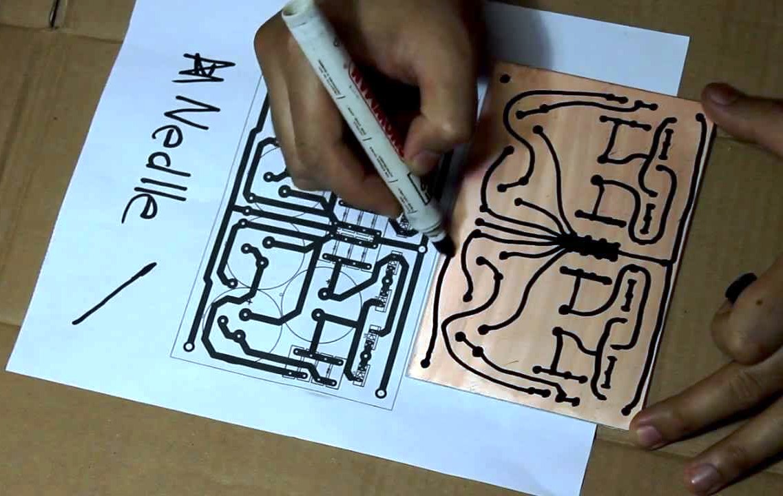
I used to harden the permanent marker tracks several times to avoid discontinuity. After that I will put that copper clad in the ferric chloride solution for etching.
Phase 2 : OrCad PCB Layout
Then one of my friend introduced me OrCad. I used OrCad PCB Layout for 3 years. Compared to my previous hand drawn experience it was really awesome. Don’t need to worry above measurements every time, just create a component footprint one then use it in as many projects.
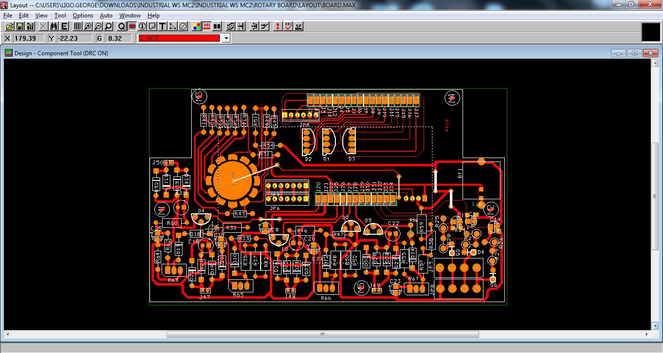
After completing the PCB design we could export the gerber files and send for PCB fabrication.
Phase 3 : Diptrace
After that I seen that some of my friends are using DipTrace. So I thought of just trying it. It was much more awesome. It was very easy and responsive to make a pcb with DipTrace compared to OrCad. I never used latest versions of OrCad as I seen that they are much more complex and sophisticated.
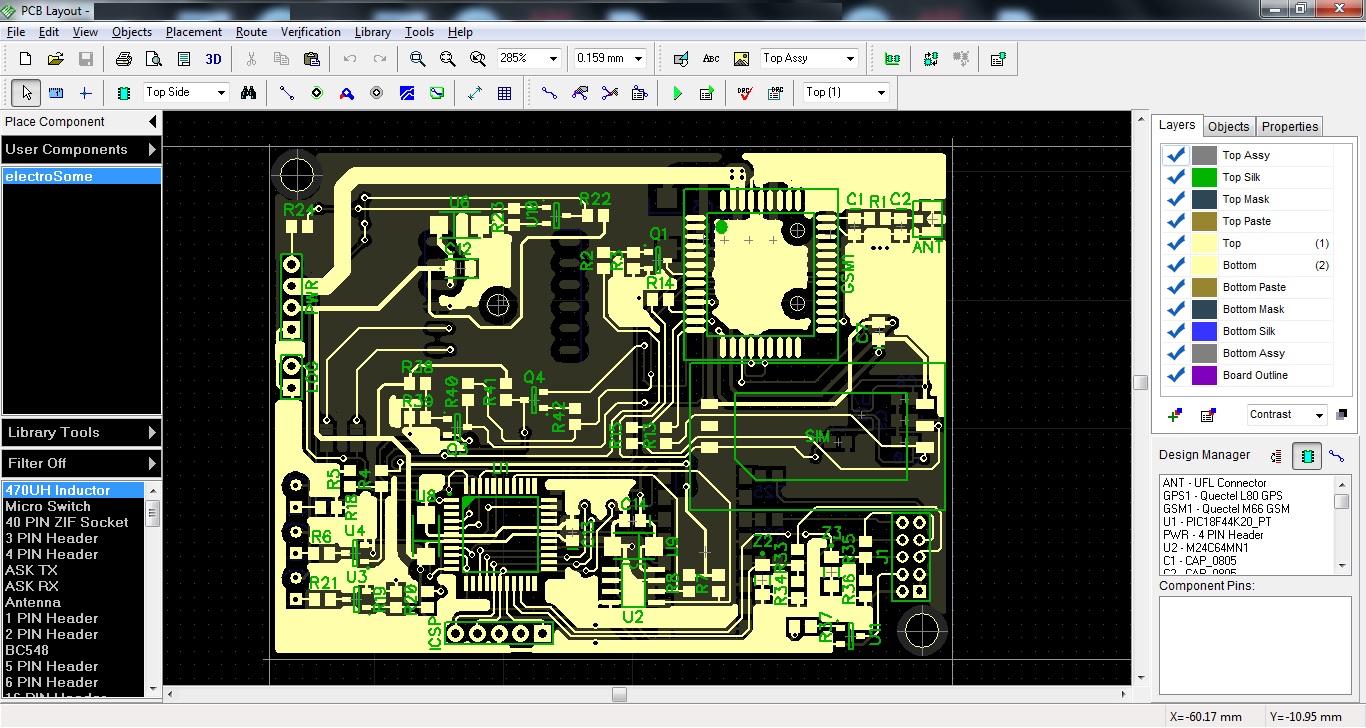
Then I realized the truth that these OrCad, Altium softwares are for designing highly completed circuits like a computer motherboard. It is highly complex and sophisticated. For beginners and medium level designs DipTrace seems to be best tool for me. (I never tried any others).
Phase 4 : EasyEDA
Then I seen that another era of design is evolving. A cloud/browser based solutions for electronics design applications. EasyEDA, Upverter, Circuit.io are leaders among these. I started using EasyEDA since it is open source. It seems to be a very nice platform for designing medium level PCBs. We don’t need to install any softwares, just need to login to a browser. Similar to checking/writing emails we can use any system/tablet/mobile which supports a modem browser.
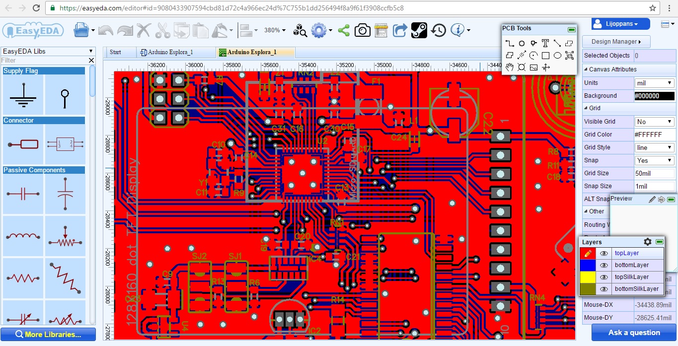
Note : I am using both Diptrace and EasyEDA nowadays. One of the problem with these cloud based solutions are that we need good internet connection. EasyEDA is developing a desktop version to solve this problem, hope that they will release it soon.
Recommended Reading : Getting Started with EasyEDA
Advantages of a Cloud Solution
- Access to a wide range of components libraries maintained by a large user base.
- No need to install any softwares
- Will work in any platforms which will support a modern browser
- Work on the go. You can work anywhere, any PC or even in mobile devices by just connecting to internet.
- No need to manually update the software. It will done automatically.
- Easily share your design with online community
- Get existing designs from the community and redesign as per our requirements
- We don’t need a good computer or laptop to do these. Just need a device which will support modern web browser.
Recommendations
EasyEDA
- Good for beginners having internet access
- Good for medium level circuits
- Work on the go in different machines
- Access to large number of libraries
DipTrace
- Good for beginners
- Good for medium level circuits (Note : Free only up to 300 pins and 2 layer)
OrCAD
- Not recommended for beginners
- Good for complex and sophisticated circuits
- It is not free
PCB Manufacturing
Ironing using Laser Print
Please read the article, “Home made PCB using Laser Print and Ironing” for more details.
Screen Printing
In the above method we transferred the print of traces to the copper clad using toner transfer method. But in this method we are using screen printing. This method is better when you need to make in bulk quantities.
Other PCB Manufacturers
I also used to manufacture PCB from MKTPCB. Nowadays a lot of manufactures are there accepting online orders, just upload the gerber file and components list.

Yes, that might be correct. You can email me at [email protected]
Try to ask google 😀 … I think, than use only simply OCR, because on the picture is texts “PCB” and “M66”.
Is it possible to share some more detail about schematic and layout of the board? Thank you.
OK good. But how google knows this image is of M66, I didn’t mention M66 anywhere in the website. Might be coincidence or their AI will be so powerful to match even a footprint in a PCB design 🙂 .
Hi, Google found 🙂 but i dont know how. To query “M66 diptrace” is the first picture. Before, than I found your website I did not know what is diptrace, so I found this picture after few minutes with “M66” and “PCB” queryss.
Hi,
I created that component in Diptrace. I wonder the way you found the M66 footprint in this article, even though this article was not about M66.
Hi, where you found the image of DipTrace? I want to make my own M66 GSM module and layout in this picture look good.