

Monostable Multivibrator using Transistors
Contents
Multivibrator is a non linear oscillator or function generator which can generate square, rectangular and pulse waves.
Monostable Multivibrator or One-Shot Multivibrator has only one stable state. By default monostable multivibrator will be in its stable state, but when triggered it will switch to unstable state (quasi-stable state) for a time period determined by the RC time constant in the circuit.
Monostable Multivibrator using Transistors – Circuit Diagram
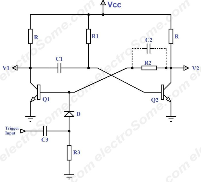
In the above circuit diagram we can find two transistors which are wired as switches. Please read the article Transistor as a Switch to know more about it. When a transistor is ON, it works in saturation region and its collector – emitter acts as a short circuit. When a transistor is OFF, it works in cut off region and its collector – emitter acts as an open circuit. So in the above circuit, when a transistor is in OFF state, its collector will have voltage equal to supply voltage Vcc and when the a transistor is in ON state, its collector will be grounded.
Function of resistor R is to limit collector current of both transistors Q1 and Q1. Resistors R1 & R2 will provide base current for transistors Q2 & Q1 respectively during ON condition. Capacitor C3 and Resistor R3 is designed as a differentiator circuit to provide sharp trigger pulses to the base of the transistor Q1. The diode D allows only positive pulses to the base. Capacitor C2 is optional, which is called as Speed Up capacitor. It is used for speedy bypassing of signal transitions (LOW to HIGH and HIGH to LOW) at the collector of Q2 to the base of Q1.
When the circuit is switched ON, transistor Q1 will be OFF and Q2 will be ON, which is its stable state. Transistor Q2 is ON since the base of the transistor is connected to Vcc via R1. Transistor Q1 will be OFF because base of the transistor is at 0v since transistor Q2 is ON.
Working
- When the circuit is switched ON, transistor Q1 will be OFF and Q2 will be ON.
- Capacitor C1 gets charged during this state.
- When a positive trigger is applied to the base of transistor Q1 it turns ON, which turns OFF the transistor Q2 due the the negative voltage from the capacitor C1.
- Capacitor C1 starts discharging during this state.
- Transistor Q1 remains in ON state due the positive voltage from the collector of transistor Q2 which is in OFF state.
- Transistor Q2 remains in OFF state until the capacitor C1 discharges compleatly.
- When the capacitor C1 discharged completly, transistor Q2 turns ON, which turns transistor Q1 OFF.
Design
R – Collector Resistor
Rc should be calculated depending upon the collector current requirement.
- Rc = ( Vcc – Vce (sat) ) / Ic
R1 – Base Resistor
R1 should be chosen such that it will provide enough collector current during saturation to the transistor Q2.
- Min. base current required, Ibmin = Ic / β, where β is the hFE of the transistor
- Safe base current, Ib = 3 Ibmin = 3Ic / β
- R1 = ( Vcc – Vbe ) / Ib
R2 – Base Resistor Q1
R2 should be chosen such that it should provide enough saturation collector current to the transistor Q1.
- R2 = (( Vcc – Vbe ) / Ib ) – R
T – Pulse Time Period
- T = 0.693R1C1
From this we can find the value of capacitor C.
Speed-Up Capacitor
Speed up capacitor is designed by considering a Compensated Attenuator composed of Base Emitter resistance of Q1, Resistor R2, Base Emitter capacitance of Q1 and seed up capacitor C2.
Base Emitter resistance of a transistor, Rπ = VT / Ib, where VT is the thermal voltage which is approximately equal to 25mV at room temperature and Ib is the base current.
Base Emitter capacitance or Input capacitance will be specified in the datasheet of the transistor. For example, the Input capacitance of BC547 transistor is 9pF.
- RπCeb = C2R2
Note 1: It may be very difficult to get the proper matching speed up capacitor but you can still use a near available one to improve the performance.
Note 2: Actually the speed up capacitor should be sized to remove the charge stored at the base of the transistor during saturation period. Unfortunately the value of Rπ and Ceb are not constant. It varies depending up on many factors. So the optimum capacitor value can be find out only through a series of experiments.
R3, C3 – Differentiator
The R3 C3 differentiator should be designed depending up on the frequency of the trigger pulse.
- R3C3 << 0.0016T’, where T’ is the lowest time period of the signal that should be differentiated.


Excellent article. Really helpful.
What would be the max input frequency range and the min. output Pulse Width for this curcuit?