

SPI – Serial Peripheral Interface
Contents
SPI (Serial Peripheral Interface) is a full duplex synchronous serial communication interface used for short distance communications. It is usually used for communication between different modules in a same device or PCB. SPI devices communicates each other using a master slave architecture with a single master. Multiple slaves are supported through individual slave select lines.
SPI Interface
SPI is called as a 4-wire bus as it requires four wires for its communication as shown below. In the case of single slave communications we need only 3 wires, as slave select (SS) is not required. So SPI requires more communication lines in contrast to UART, I2C, USB etc.
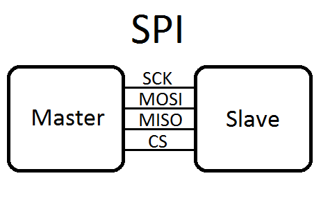
- SCK or SCLK : Serial Clock, clock generated by master
- MOSI or SDO : Master Output Slave Input, data output from master
- MISO or SDI : Master Input Slave Output, data output from slave
- SS : Slave Select, often an active low input of a slave
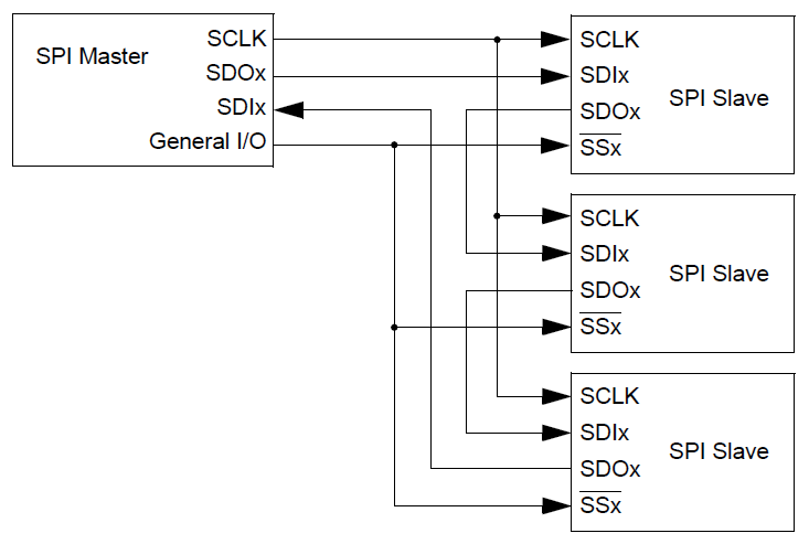
When multiple slave devices are used, an independent slave select line is connected from master to each slave device as below.
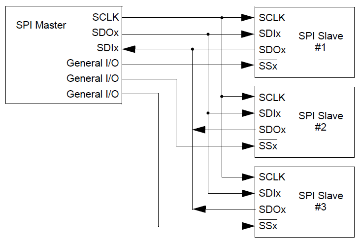
Master will select only one slave at a time. Mostly slave devices will be equipped with tri-state outputs. So when they are not selected, their output lines appears disconnected.
SPI Device
Hope you got the basic idea of an SPI bus. Now let’s see in little more detailed level like how it is working in hardware level. SPI having relatively very simple hardware compared to other serial communication protocols like UART, I2C etc. Its operation is based on shift registers (usually 8 bit). Each devices (master and slave) uses shift registers to shift data in and out of the system.
For the sake of explanation here we can considering only a single slave device.
Hardware
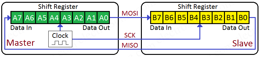
As you can see above shift registers in the master and slave devices are connected together such that it forms a circular buffer. These registers operate in Serial In/Serial Out (SISO) mode. Output of a register is connected to the input of another register and vice versa. You can see that the clock signal is generated by the master device.
Working of SPI

You can easily understand the working from the above animation. Master will generate clock whenever it wants to write data to a Slave device. After 8 clock pulses data in the master device (A7 ~ A0) is transferred to slave device and data in the slave device (B7 ~ B0) is transferred to the master device.
Buffer
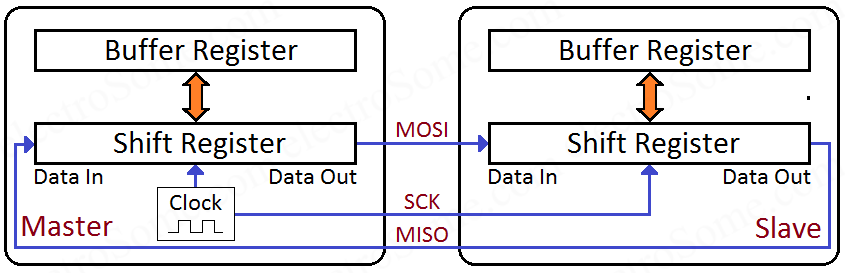
For the sake of explanation, I omitted Buffer Register. It acts as an interface between user (processor, programmer) and SPI. Usually shift register won’t be directly accessible. So if we need to transmit data, we will write it to the buffer register. So it will automatically written to shift register when it is free and transmission will start. Similarly data is received in the shift register is automatically transferred to buffer register once the reception is complete. We can easily read from it. Thus buffer register will avoid all glitches that can happen if we try to read or write to shift register directly while transmission is taking place.
SPI Modes – Clock Polarity & Phase
We already seen that clock for data transfer is generated by the SPI master. So the master should set the clock frequency for SPI transfer. In addition to this clock polarity and clock phase are there, which has to match with SPI slaves for proper data transfer.
- Clock Polarity : CPOL or CKP
Clock polarity is the idle / active state of the clock. If idle state is 0, active state will be 1 and vice versa. - Clock Phase : CPHA, Inverted Clock Phase (Clock Edge) : NCPHA or CKE
Clock phase or clock edge defines when to transfer data. Data can be transferred during LOW (0) to HIGH (1) or HIGH to LOW transitions.
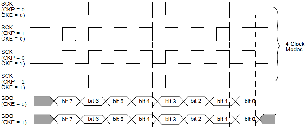
- Clock Polarity (CKP) = 0
This means that the base value of clock is zero. Which implies idle state is 0 and active state is 1.- Clock Edge (CKE) = 0
Data transmission occurs during idle to active clock state, ie LOW to HIGH transition. - Clock Edge (CKE) = 1
Data transmission occurs during active to idle clock state, ie HIGH to LOW transition
- Clock Edge (CKE) = 0
- Clock Polarity (CKP) = 1
This means that the base value of clock is one. Which implies idle state is 1 and active state is 0.- Clock Edge (CKE) = 0
Data transmission occurs during idle to active clock state, ie HIGH to LOW transition. - Clock Edge (CKE) = 1
Data transmission occurs during active to idle clock state, ie LOW to HIGH transition.
- Clock Edge (CKE) = 0
So these different clock configurations can be considered as different modes of SPI as below.
| SPI Mode | Clock Polarity | Clock Edge/Phase | |
|---|---|---|---|
| CPOL/CKP | CPHA | NCPHA/CKE | |
| 0 | 0 | 0 | 1 |
| 1 | 0 | 1 | 0 |
| 2 | 1 | 0 | 1 |
| 3 | 1 | 1 | 0 |
Configurations
Independent Slave Configuration
In the independent slave configuration, there is an independent slave select line from master to each slave. SPI is commonly used in this way. SPI slave output (SDOx or MISO) will be a tri-state pin, so it will be in high impedance state when the slave is not selected. In this configuration master can select any slave device and start communication as per requirements.
Daisy Chain Configuration
In this configuration SPI can be connected one after another in a serial form. In this configuration a single slave select line is used to select all daisy chain slaves. Whole chain acts like a communication through shift registers connected in series. Each daisy chain slave is supposed to send out exact copy of data received in the first group of clock cycles during the second group of clock cycles.
This configuration is commonly used in JTAG.
Tips
How a Master read data from a Slave ?
As you see above SPI communication is always full duplex. Master will generate clock only when it needs to write data to a slave device. So for reading data from a slave device we can just send a dummy data to slave device.
Do you Know ?
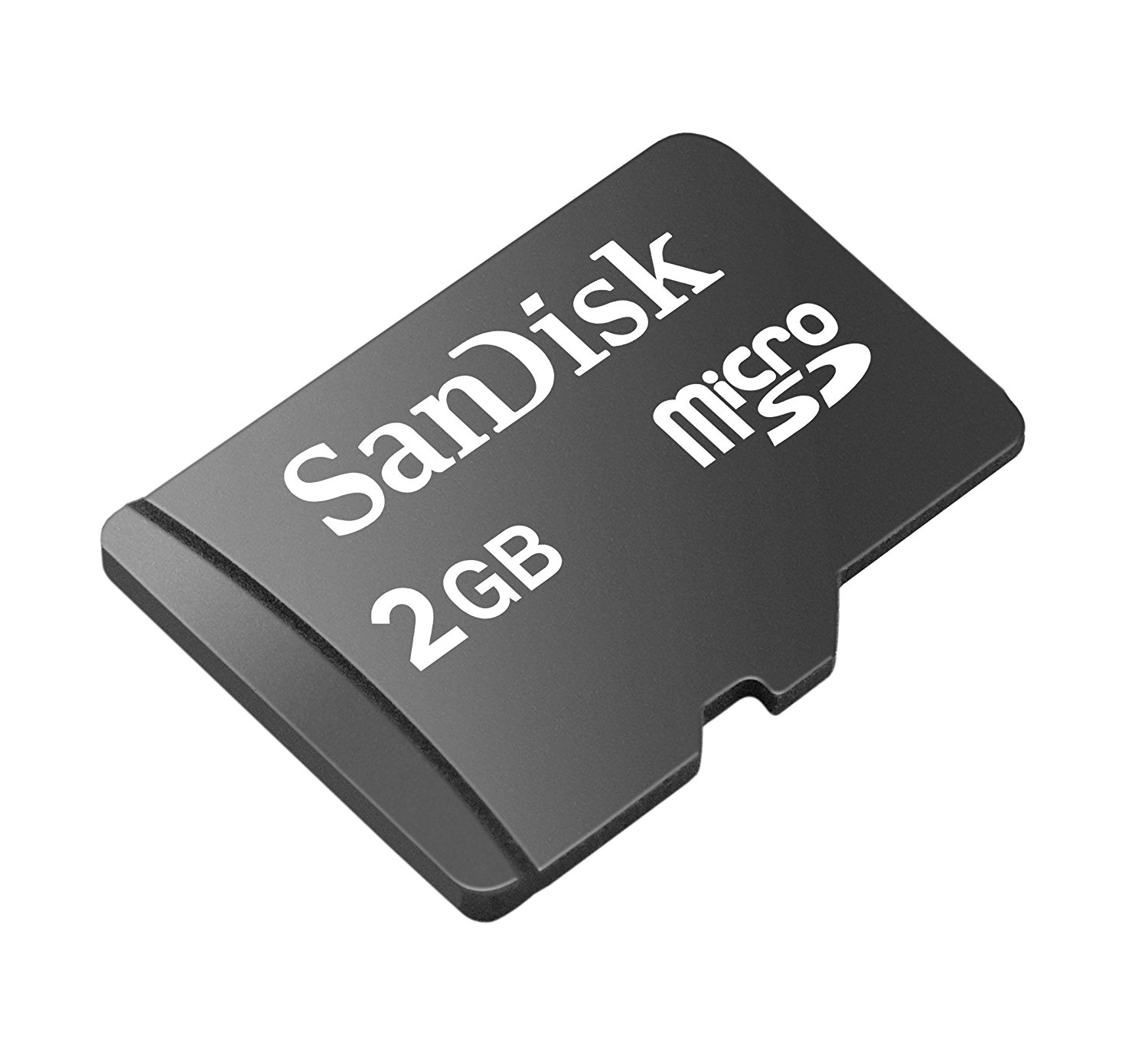
SD Cards and MicroSD cards uses SPI protocol for data transfer.
Pros and Cons
Advantages
- Simple hardware
- Full duplex communication
- Simple software implementation
- High Speed
- No speed limit (practically it will be limited by the clock frequency, rise time, fall time etc.)
- Not Limited to 8 bit data
- Signals are unidirectional through all lines, makes easy isolation
- No need of unique address in slaves like in RS485 or I2C.
- No need of precision oscillators in slave devices as it uses master’s clock
- No complex transceivers are required
Disadvantages
- More pins/wires are required. Minimum 3 wires (in single slave) are required.
- Can be used only from short distances
- No error detection protocol is defined
- Usually supports only one master
Applications
- SD Cards
- LCD Displays
- RTC
- Ethernet Controllers


good explanation^-^!!!!
is useful…interesting