

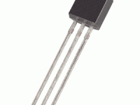
Transistor as a Switch
Contents
We all know that a transistor has 4 regions of operation, in which Active, Cutoff and Saturation are commonly used. A transistor works in active region when worked as an Amplifier. When a transistor works as a Switch it works in Cutoff and Saturation Regions. In the Cutoff State both Emitter Base Junction and Collector Base junctions are reverse biased. But in saturation region both junctions are forward biased. Switch is a very useful and important application of transistors. In most digital IC’s transistors will work as a switch to make power consumption very low. It is also a very useful circuit for an electronics hobbyist as it can be used as a driver, inverter etc..
Circuit Diagram – Transistor as a Switch

From the above circuit we can see that the control input Vin is given to base through a current limiting resistor Rb and Rc is the collector resistor which limits the current through the transistor. In most cases output is taken from collector but in some cases load is connected in the place of Rc.
- ON = Saturation
- OFF = Cutoff
Transistor as a Switch – ON

Transistor will become ON ( saturation ) when a sufficient voltage V is given to input. During this condition the Collector Emitter voltage Vce will be approximately equal to zero, ie the transistor acts as a short circuit. For a silicon transistor it is equal to 0.3v. Thus collector current Ic = Vcc/Rc will flows.
Transistor as a Switch – OFF

Transistor will be in OFF ( cutoff ) when the input Vin equal to zero. During this state transistor acts as an open circuit and thus the entire voltage Vcc will be available at collector.
Design
Collector Current, Ic = ßIb + Iceo
where ß is the gain in common emitter configuration and lceo is the leckage current.
Leackage current, Iceo can be neglected, so
Ib = Ic/ß
When the transistor is ON ( saturation region ), the collector emitter voltage Vce is approximately equal to zero. For a silicon transistor it usually 0.3v. So collector current Ic can be written as,
Ic = (Vcc – Vce)/Rc, which is the maximum Ic that can flow through the circuit.
Ic = Vcc/Rc, since Vce is less than 0.3V.
To keep transistor in saturation enough base current Ib must flow. The minimum base current can be find out from the equation Ib = Ic/ß
To ensure that the transistor is in saturation we will take Ib’ = 10Ib
So Rb = (Vin – Vbe)/Ib’
Note : In the case of a PNP transistor just replace GND with Vcc , Vcc with GND and the transistor will be ON when the input voltage Vin is LOW.
Different Ways of Connecting Loads
Load can be connected to transistor in different ways, some of them are shown below.

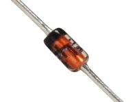
In the case of inductive loads such as Relay a freewheeling diode should be connected in parallel to it.
Calculate Base Resistance Value
Nice article. It’s very helpful to me. Please keep sharing.
It’s for hobbyist ? I thought that, even if it’s a simple circuit, it leads to osscilators, digital circuits and to assembly language. It seems to be learned by future professional. I hope so.
I love this post undoubtely, anyway.