

Using ADC of PIC Microcontroller – MPLAB XC8
Contents
In this tutorial we will learn, how to use the ADC module of a PIC Microcontroller using MPLAB XC8 compiler. For demonstration we will use the commonly available PIC 16F877A microcontroller.
Every physical quantity found in nature like temperature, humidity, pressure, force is analog. We need to convert these analog quantities to digital to process it using a digital computer or a microcontroller. This is done by using Analog to Digital Converters. An Analog to Digital Converter or ADC is a device which converts continuous analog quantity (here : voltage) to corresponding discrete digital values.
PIC 16F877A microcontroller has 8 ADC inputs and it will convert analog inputs to a corresponding 10 bit digital number. For the sake of explanation take ADC Lower Reference as 0V and Higher Reference as 5V.
- Vref- = 0V
- Vref+ = 5V
- n = 10 bits
- Resolution = (Vref+ – Vref-)/(2n – 1) = 5/1023 = 0.004887V
So ADC resolution is 0.00487V, which is the minimum required voltage to change a bit. See the examples below.
| Analog Input | Digital Output | ||
|---|---|---|---|
| Binary | Hex | Decimal | |
| 0 | 0b0000000000 | 0x000 | 0 |
| 0.004887V | 0b0000000001 | 0x001 | 1 |
| 0.009774V | 0b0000000010 | 0x002 | 2 |
| 0.014661V | 0b0000000011 | 0x003 | 3 |
| 4.999401V | 0b1111111111 | 0x3FF | 1023 |
The ADC module of PIC 16F877A has 4 registers.
- ADRESH – A/D Result High Register
- ADRESL – A/D Result Low Register
- ADCON0 – A/D Control Register 0
- ADCON1 – A/D Control Register 1
ADC Block Diagram
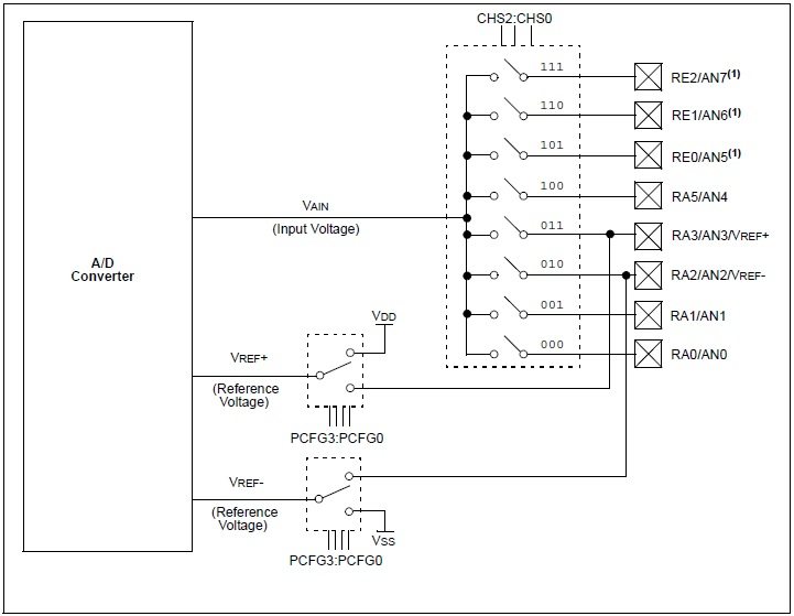
From this block diagram you can easily understand the working of ADC channel selection and reference voltage selection.
ADCON0 – A/D Control Register 0
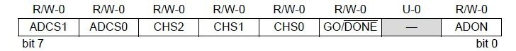
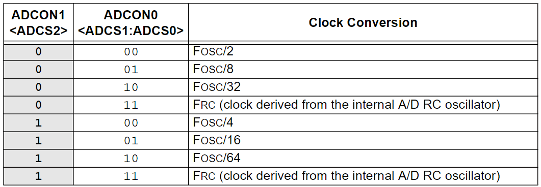
- Bit 7 ~ 6 : ADCS1 & ADCS0, A/D Conversion clock selection bits. These bits are used in combination with ADCS2 of ADCON1 register. (See the ADC Clock Selection Table)
- Bit 5 ~ 3 : CH2, CH1 & CH0 are analog channel selection bits which will select a particular channel out of 8.
- Bit 2 : Go_nDone is the A/D conversion status bit. Setting this bit initiates the A/D conversion and it will be automatically cleared when the conversion completes.
- Bit 1 : Unimplemented, Read as 0.
- Bit 0 : ADON, A/D Module On bit. Setting this bit will turn on the ADC module.
ADCON1 – A/D Control Register 1
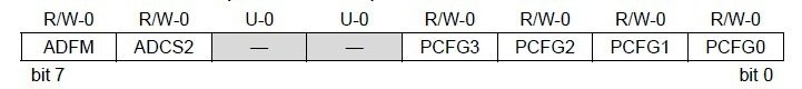
- Bit 7 : ADFM, A/D Result Format bit. Bits of result will be right justified if this bit is set otherwise it will be left justified.
- Bit 6 : ADCS2, A/D Conversion clock selection bit. This bit is used in combination with ADCS0 and ADCS1 of ADCON0 register. (See the ADC Clock Selection Table)
- Bit 5 ~ 4 : Unimplemented. Read as 0.
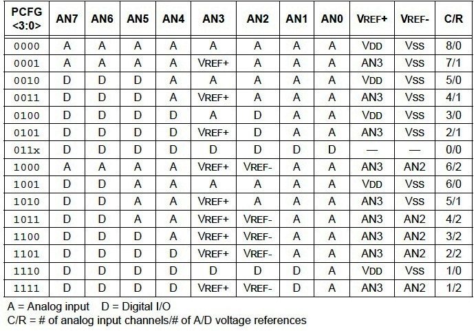
- Bit 3 ~ 0 : PCFG3 ~ PCFG0, A/D Port Configuration Bits. Status of these bits determine whether the pin is Analog or Digital as per the table below.
Note : Some ICs use special register ANSEL for setting each pin as analog or digital.
A/D Acquisition Time
Holding capacitor (CHOLD) must be charged to the input voltage to meet the accuracy specified by the datasheet. So we must provide a delay greater than the minimum required acquisition time to charge the capacitor. 19.72μs is the minimum time specified in the datasheet. Please refer the datasheet for more details.
A/D Clock Selection
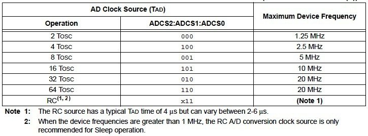
A/D conversion clock must be selected to ensure minimum TAD. TAD is the conversion time per bit, which is 1.6μs. Please refer the datasheet for more details.
Circuit Diagram
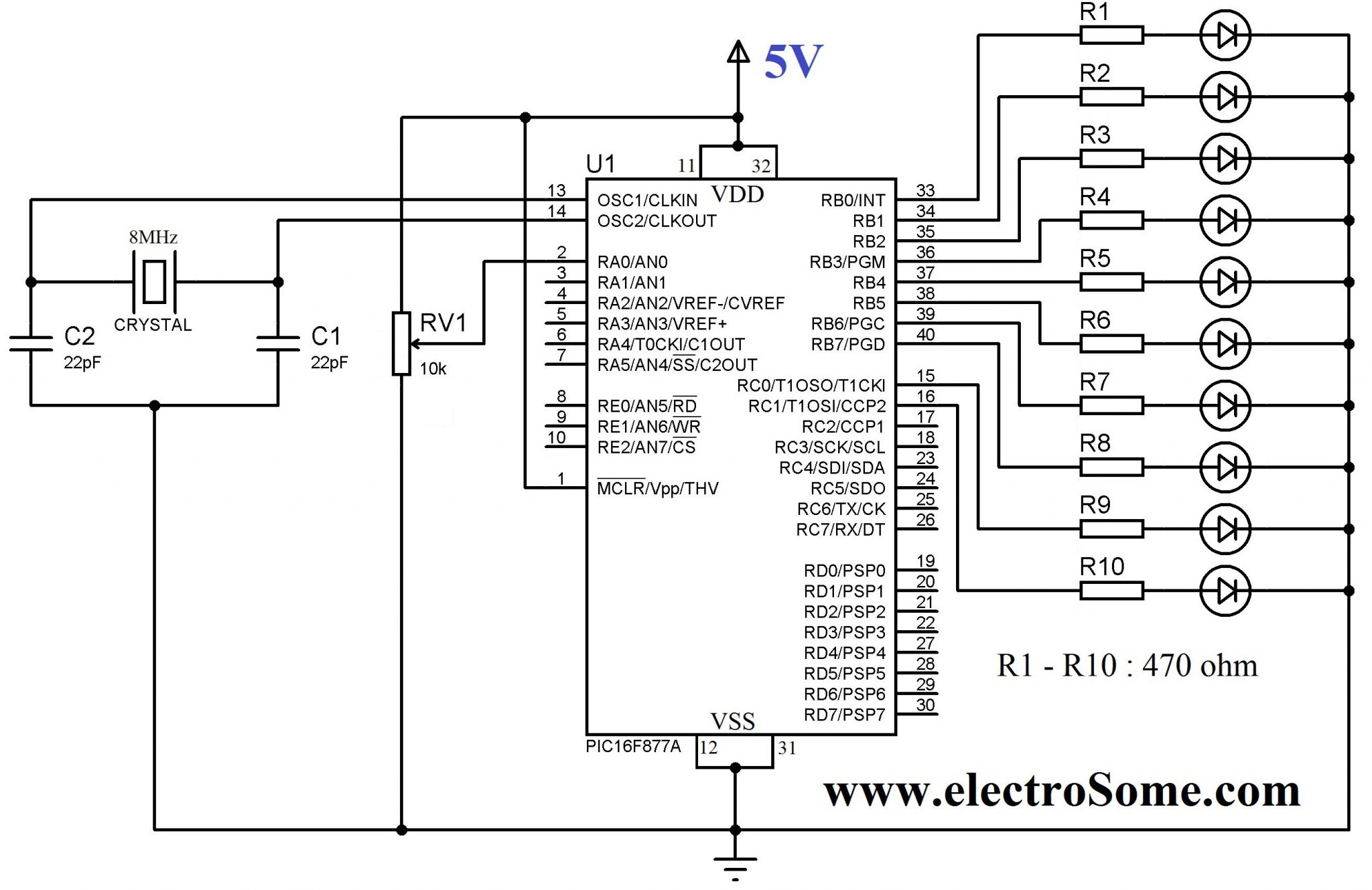
You can easily understand the circuit if you already go through our first tutorials, PIC Microcontroller MPLAB XC8 Tutorials. The reference voltages for A/D conversion is set to VDD (5V) and VSS (GND) in the software (see the code below). Analog input to Channel 0 is provided using a potentiometer such that we can vary the input voltage from 0 ~ 5V. A/D conversion will generate a 10 bit digital value (0 ~ 1023) corresponding to the analog input. This digital value is displayed using 10 LEDs connected PORTB and PORTC of the microcontroller.
MPLAB XC8 Code
// CONFIG
#pragma config FOSC = HS      // Oscillator Selection bits (HS oscillator)
#pragma config WDTE = OFF     // Watchdog Timer Enable bit (WDT disabled)
#pragma config PWRTE = OFF    // Power-up Timer Enable bit (PWRT disabled)
#pragma config BOREN = OFF    // Brown-out Reset Enable bit (BOR disabled)
#pragma config LVP = OFF      // Low-Voltage (Single-Supply) In-Circuit Serial Programming Enable bit (RB3 is digital I/O, HV on MCLR must be used for programming)
#pragma config CPD = OFF      // Data EEPROM Memory Code Protection bit (Data EEPROM code protection off)
#pragma config WRT = OFF      // Flash Program Memory Write Enable bits (Write protection off; all program memory may be written to by EECON control)
#pragma config CP = OFF       // Flash Program Memory Code Protection bit (Code protection off)

#include <xc.h>
#include <pic16f877a.h>

#define _XTAL_FREQ 8000000

void ADC_Init()
{
  ADCON0 = 0x81;               //Turn ON ADC and Clock Selection
  ADCON1 = 0x00;               //All pins as Analog Input and setting Reference Voltages
}

unsigned int ADC_Read(unsigned char channel)
{
  if(channel > 7)              //Channel range is 0 ~ 7
    return 0;

  ADCON0 &= 0xC5;              //Clearing channel selection bits
  ADCON0 |= channel<<3;        //Setting channel selection bits
  __delay_ms(2);               //Acquisition time to charge hold capacitor
  GO_nDONE = 1;                //Initializes A/D conversion
  while(GO_nDONE);             //Waiting for conversion to complete
  return ((ADRESH<<8)+ADRESL); //Return result
}

void main()
{
  unsigned int a;
  TRISA = 0xFF;                 //Analog pins as Input
  TRISB = 0x00;                 //Port B as Output
  TRISC = 0x00;                 //Port C as Output
  ADC_Init();                   //Initialize ADC

  do
  {
    a = ADC_Read(0);            //Read Analog Channel 0
    PORTB = a;                  //Write Lower bits to PORTB
    PORTC = a>>8;               //Write Higher 2 bits to PORTC
    __delay_ms(100);            //Delay
  }while(1);                    //Infinite Loop
}
I hope that the program is self explanatory as it is well commented.
Download Here
You can download the complete zipped project folder here.
I hope that you understand everything what I explained. Please do a comment if you have any doubt, which will help me to improve this tutorial.


1. ADC_Read() function is a general function. This just an example program. You may use other ADC channels if required. Other channels are not used in this program.
2. This is done just to make ADC_Read() a general function.
3. It is not for changing justification. One register in this microcontroller holds only 8bits. I guess this MCU is having 10bit ADC. So it just combines ADC result registers to a single value.
I have a few queries.
1. channel is always going to be 0. Therefore what is the necessity to check if channel >7 in the ADC_read() ?
2. Subsequently, what is the function of resetting the channel bits and setting them again in the next two lines. Can we not configure this permanently in the ADCON1 and ADCON0 registers?
3. Also, is my understanding accurate as regarding to the 8 right shifts you do when returning the result of ADC_read() is to change justification of the ADC result? Can this not be achieved by setting ADFM ( ADCON1.7) =1 [which means right justified]
Thank you for the wonderful content. This is Very helpful.
Check the datasheet sir.
Thanks for your feedback.
Thanks a lot respected Mr George for well commented program. It is very useful.
With Regards,
S S RANA
ADCON0 &= 0xC5; is equivalent to
ADCON0 = ADCON0 & 0xC5; (ADCON0 & 1011 0101)=>( 1000 0001 & 1011 0101)
ADCON0 |= channel<<3; is equivalent to
ADCON0= ADCON0 | (channel< ADCON0 | (0000 0000< (1000 0001 | 0000 0000)
{i.e if channel is 1 then => ADCON0 | {0000 0001< (1000 0001 | 0000 1000) }
Hope it helps
Where can i find the ?
Hi! I have a little problem. I write a loop to read the ADC channel 0 every 500ms, but the ADC change the result sometimes. I put the AN0 input on 0V and the ADC continue doing this. The great problem is the result, it’s many bits of error. Could you help me to know what happen?
what’s different between this pic (16f877) and 18f45k22? I traied to use your code with some little changes for my pic but it doesn’t work…Could you help me?
For anyone wondering why their code only showing zeroes for the lower 6 bits, it’s because you are copy and pasting the code on this page which is left justified. Simply change ADCON1 to 0x80 to fix this.
thank you sir…i’ll contact you with my query..:)
Hello , I have the same question ! what should we change that it can work for the pic18F
I think (ADRESH<<8)+ADRESL works for ADFM=1?
I must be missing something
(ADRESH<<8)+ADRESL)?
Please help me understand, i can see ADFM=0 and how the result is left justified.
Shouldnt the result be (ADRESH<>6)?
*(ADRESH<>6) = moving the lowest from bits 7-6 to 1-0 so they add onto the gaps made by ADRESH<<2.
Thanks btw this was very helpful.
Can some one explain
I cant understand these two lines.
ADCON0 &= 0xC5; //Clearing the Channel Selection Bits
ADCON0 |= channel<<3; //Setting the required Bits
that is only a 1 bit problem. That might be caused due to some voltage issue. A difference of 0.004887V can cause it. Nothing to worry about it.
Hey, i have a problem with RB0 bit. My hardware and software are exactly the same, but RB0 is always inverted result, when analogue input is 5V, all leds light up except RB0, at the other end when input is 0, only RB0 is HIGH, any idea whats happening? Already tried with disabling interupt register INTCONbits.INTE = 0;
Above article is about using internal ADC of pic microcontroller not adxl335.
Please use our forums ( https://electrosome.com/forums/ ) for asking doubts outside the scope of above article.
sir ,how calculate adxl335 out put
You can easily convert and use it for 18F4520 if you clearly understand above program.
Please let us know if you want any premium support. Mail me at [email protected]
You may also use our forums ( https://electrosome.com/forums ) if you need any free support outside the scope of above article.
how would we do this for PIC18F4520
Hi,
You can use this article as a reference : https://electrosome.com/thermometer-pic-microcontroller-lm35/
thanks for your reply……
bro actually i planned to build temperature sensor using mplab x and lm35…….how to convert the lm35 reading to actual value….i tried with above one by using adc= ((ADC_value*5)/1024); but it’s not working help me bro
Check the channel selection bits of ADCON0. Anding with 0xC5 will make all the channel selection bits zero.
thanks for explanation but one small doubt
ADCON0 &= 0xC5; //Clearing channel selection bits
ADCON0 |= channel<<3; //Setting channel selection bits
__delay_ms(2); //Acquisition time to charge hold capacitor
GO_nDONE = 1; //Initializes A/D conversion
while(GO_nDONE); //Waiting for conversion to complete
return ((ADRESH<<8)+ADRESL); //Return result
why u used & AND symbol and OR symbol in ADCON0 and return statement also?i am poor in coding will u help me pls
and also displaying value of a into high and low bit?
You can calculate the required acquisition time and provide some delay greater than it.
Thank you very much for a great explanation. This is the first time that I’ve seen an ADC function carried out using the __delay function, which seems a great idea. However, I’ve not been able to understand why you delay 2ms. Would it not be more efficient to delay, say 22us? Or have I misunderstood the A/D Acquisition time element?